

Panasonic AN8814SB Datasheet
ICs for Compact Disc/CD-ROM Player
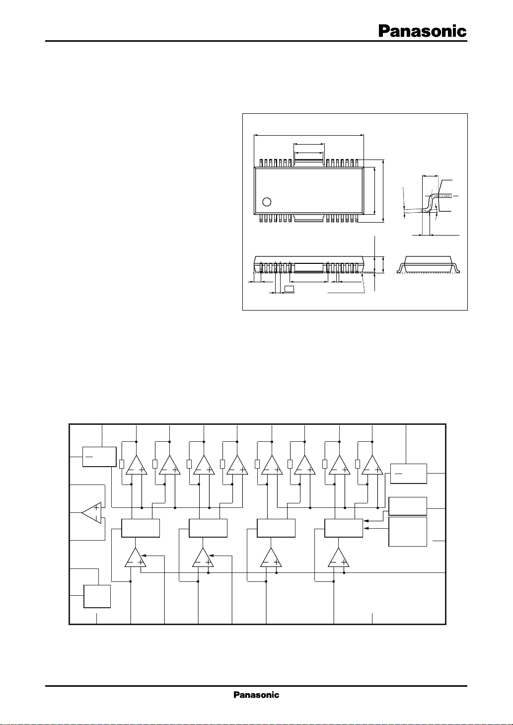
AN8814SB
4-channel driver IC for optical disk drive
■ Overview
The AN8814SB is a BTL system 4-channel
driver and is encapsulated in the SMD package
which excels in heat radiation characteristic.
■ Features
• Wide output dynamic range regardless of refer-
ence voltage of the system
• Driver I/O gain setting is possible with an addi-
tional external resistor
• 3.3 V supply voltage is available due to an exter-
nal PNP-tr.
• Additional OP-amp. built-in
■ Applications
• MD, CD/CD-ROM drive
• DVD/DVD-ROM drive
■ Block Diagram
CC1
PV
20
18
VO1+
17
VO1−
VO2+
16
18.4±0.2
(5.15)
28 22 21
17 814
(1.2)
(4.8)
(6.4)
0.8
Seating plane
HSOP042-P-0400
VO2−
15
14
VO3+
VO3−
13
12
0.35
VO4+
+0.10
–0.05
Unit: mm
15
(1.315)
–0.05
+0.10
8.3±0.22.7±0.20.1±0.1
10.93±0.30
0.30
0° to 10°
0.65±0.20
CC2
VO4−
11
PV
9
21
1
PV
CC
2
1
PV
6
4
Direction
5
V
CC
detector
Direction
detector
Direction
detector
Direction
detector
2
V
detector
Thermal
protection
circuit
1
2
3.3 V
CC
CC
Fin
8
7
22
V
CC
GND
V
REF
reg.
19
PGND1
23
24
IN1
PC1
25
IN2
26
PC2
27
IN3
28
10
IN4
PGND2
1

AN8814SB ICs for Compact Disc/CD-ROM Player
■ Pin Descriptions
Pin No. Description
1 Base control pin for an external transistor
of 3.3 V regulator
2 3.3 V regulator output monitor pin
3 N.C. pin
4 Op-amp. output pin
5 Op-amp. inverted input pin
6 Op-amp. non-inverted input pin
7 Power supply pin
8 1/2 PVCC output pin 2
9 Driver power supply pin 2
10 Driver GND pin 2
11 Motor driver-4 reverse rotation output pin
12 Motor driver-4 forward rotation output pin
13 Motor driver-3 reverse rotation output pin
14 Motor driver-3 forward rotation output pin
Pin No. Description
15 Motor driver-2 reverse rotation output pin
16 Motor driver-2 forward rotation output pin
17 Motor driver-1 reverse rotation output pin
18 Motor driver-1 forward rotation output pin
19 Driver GND pin 1
20 Driver power supply pin 1
21 1/2 PVCC output pin 1
22 V
input pin
REF
23 Motor driver-1 input pin
24 PC (power cut) input pin 1
25 Motor driver-2 input pin
26 PC (power cut) input pin 2
27 Motor driver-3 input pin
28 Motor driver-4 input pin
Fin GND pin
■ Absolute Maximum Ratings
Parameter Symbol Rating Unit
Supply voltage SV
Supply current I
2
Power dissipation
Operating ambient temperature
Storage temperature
Note)*1: Except for the operating ambient temperature and storage temperature, all ratings are for Ta = 25°C.
2: Ta = 85°C.
*
Referring to "■ Application Circuit Example", following the allowable power dissipation characteristic curve of "■
Application Notes".
*
1
*
1
*
CC
CC
P
D
T
opr
T
stg
17 V
mA
542 mW
−30 to +85 °C
−55 to +150 °C
■ Recommended Operating Range
Parameter Symbol Range Unit
Supply voltage SVCC , PV
CC1
, PV
CC2
4.0 to 14 V
2
 Loading...