

Panasonic AN8783SB Datasheet
ICs for Compact Disc/CD-ROM Player
AN8783SB
4-channel linear driver IC for CD/CD-ROM drive
■ Overview
The AN8783SB employs one channel of power
op-amp. system and three channels of H-bridge
system. Two channels out of three channels of Hbridge method are a current feedback system. So
this IC is optimum for driving an actuator and a
motor of CD/CD-ROM drive. It comes with a
surface mount package which excels in a heat radiation characteristic.
■ Features
• Little phase delay due to current feedback system
(2-channel for actuator)
• 4 modes of forward, reverse rotations, braking and
standby can be selected from channels for loading motor (H-bridge method) by a digital signal
from a microcomputer.
• Wide output dynamic range regardless of refer-
ence voltage of the system
• Setting the input level of a driver by an external
resistor is possible.
• PC (power cut) function built-in (common for ch.
1, ch. 3 and ch. 4)
• Thermal shut-down circuit built-in (with hyster-
esis)
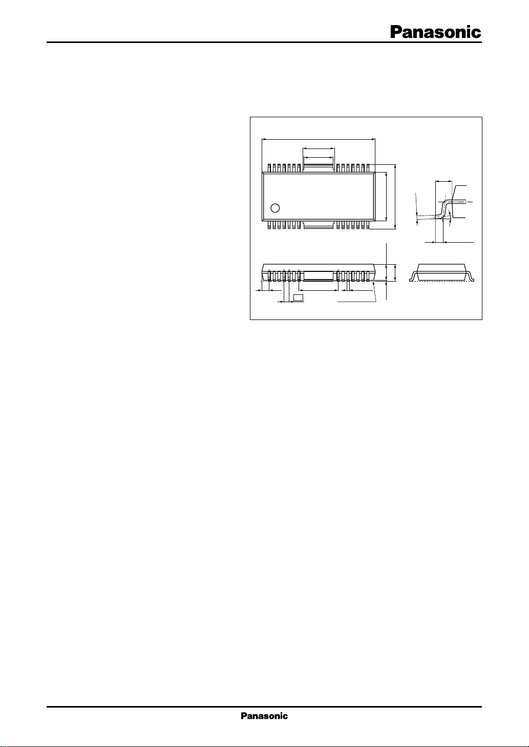
18.4±0.2
(5.15)
28 22 21
17 814
(1.2)
(4.8)
(6.4)
0.8
15
8.3±0.22.7±0.20.1±0.1
+0.10
0.35
–0.05
Seating plane
HSOP042-P-0400
+0.10
10.93±0.30
Unit: mm
(1.315)
–0.05
0.30
0° to 10°
0.65±0.20
■ Applications
• CD/CD-ROM drive
1
AN8783SB ICs for Compact Disc/CD-ROM Player
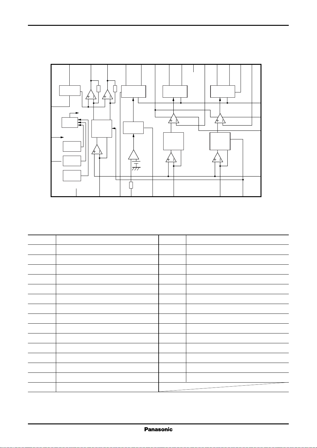
■ Block Diagram
PGND1
19
28
Fin
21
1/2 PV
Reset
SV
Thermal
protect
SV
monitor
V
monitor
PVC1
CC
CC
REF
CC
27
D1+
20
18
ch. 1 ch. 2
Direction
det.
current
amp.
N.C.
IN1
D1−
D2−
17
BTL linear
driver ch. 2
Control
252324
AS
■ Pin Descriptions
Pin No. Description
1 PC1 (power cut) input pin
2 Driver-3 phase compensation pin
3 Driver-3 input pin
4 Driver-4 input pin
5 Driver-3 feedback pin
6 Driver-4 feedback pin
7 Driver-4 phase compensation pin
8 Driver-4 current feedback power supply pin
9 Driver-4 reverse rotation output pin
10 Driver-4 forward rotation output pin
11 Driver-2, driver-4 GND pin
12 Driver-3 reverse rotation output pin
13 Driver-3 current feedback power supply pin
14 Driver-3 forward rotation output pin
15 Driver-2 forward rotation output pin
logic
IN2
D2+
15
Comp.
D3+
16
26
PC2
PVC2
BTL linear
driver ch. 3
Absolute
direction
14
V-l
det.
3
IN3
D3−
12
ch. 3
PVC3
13
5
Absolute
direction
D4+
10
BTL linear
driver ch. 4
V-l
det.
4
Pin No. Description
16 Driver-2 power supply pin
17 Driver-2 reverse rotation output pin
18 Driver-1 reverse rotation output pin
19 Driver-1 GND pin
20 Driver-1 forward rotation output pin
21 Driver-1 power supply pin
22 V
input pin
REF
23 Driver-1 input pin
24 Driver-2 input pin
25 Driver-2 output voltage adjustment pin
26 PC2 (power cut) input pin
27 N.C.
28 Power supply pin
Fin GND pin
9
ch. 4
IN4
D4−
PVC4S3S4
8
1
PC1
6
11
PGND2
7
2
22
V
REF
2
ICs for Compact Disc/CD-ROM Player AN8783SB
■ Absolute Maximum Ratings
Parameter Symbol Rating Unit
Supply voltage SV
Supply current I
2
Power dissipation
Operating ambient temperature
Storage temperature
Note)*1: Except for the operating ambient temperature and storage temperature, all ratings are for Ta = 25°C.
2: Referring to "■ Application Circuit Example", use within the range of PD = 542 mW or less at Ta = 85°C, following the
*
allowable power dissipation characteristic curve of "■ Application Notes".
*
1
*
1
*
CC
CC
P
D
T
opr
T
stg
■ Recommended Operating Range
Parameter Symbol Range Unit
Supply voltage SV
CC
PVC1 , PV
C2
14.4 V
mA
542 mW
−30 to +85 °C
−55 to +150 °C
6.4 to 14 V
4.5 to 14
■ Electrical Characteristics at SVCC = 12 V, V
= 12 V, V
CC1
Ta = 25°C
Parameter Symbol Conditions Min Typ Max Unit
= I
= I
Current consumption 1 with no I
SVCCIIN1
IN3
signal
Current consumption 2 with no I
VCC1IIN1
= I
IN3
signal
Current consumption 3 with no I
VCC2IIN1
= I
IN3
signal
Driver 1
Output offset voltage V
Gain (+)G
Relative gain (+/−) ∆G
Limit voltage (+)V
Limit voltage (−)V
OOF-1
1+
1−
L1+
L1−
Driver 2
Output voltage 1 (+)V
21+VPC1
= 5 V, V
RAS = 10 kΩ
Output voltage 1 (−)V
21−VPC1
= 5 V, V
RAS = 10 kΩ
Output voltage 2 (+)V
22+VPC1
= 5 V, V
RAS = 0 kΩ
Output voltage 2 (−)V
22−VPC1
= 5 V, V
RAS = 0 kΩ
= 0 µA 15 30 mA
IN4
= I
= 0 µA 46mA
IN4
= I
= 0 µA 14mA
IN4
PC2
PC2
PC2
PC2
CC2
= 0 V, V
= 0 V, V
= 0 V, V
= 0 V, V
= 5 V, RL = 8 Ω, V
= 0 V, V
PC1
PC2
−30 0 30 mV
18.5 21.0 23.5 dB
−3.0 0 3.0 dB
6.5 8.0 V
−8.0 −6.5 V
= 1 V, 2.4 2.7 3.0 V
IN2
= 4 V, −3.0 −2.7 −2.4 V
IN2
= 1 V, 3.4 4.0 V
IN2
= 4 V, −4.0 −3.4 V
IN2
= 5 V,
3
 Loading...