

Voltage Regulators
AN8016NSH
Single-channel 1.8-volt step-up DC-DC converter control IC
■ Overview
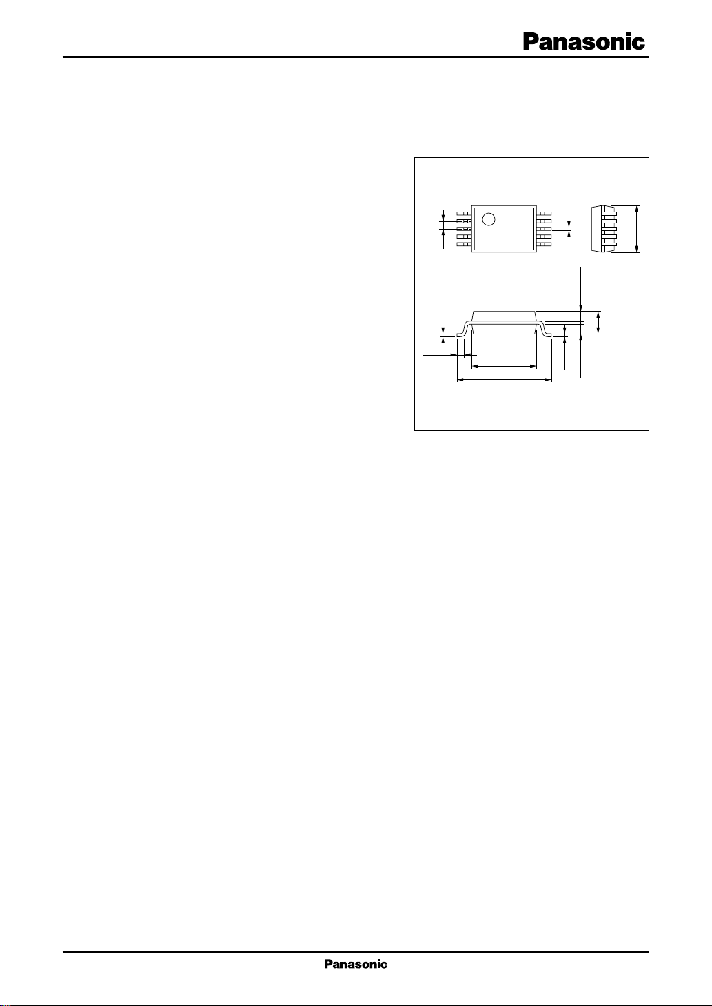
Unit: mm
The AN8016NSH is a single-channel PWM DC-DC
converter control IC that supports low-voltage operation.
This IC allows a stepped-up voltage output to be provided with a minimal number of external components. It
features a low minimum operating voltage of 1.8 V, and
1
5
0.5
10
0.2±0.1
6
due to being provided in a 10-pin surface mount package
with a 0.5 mm lead pitch, is optimal for use in miniature
+0.1
–0.05
0.15
0.625±0.100.625±0.10
1.5±0.2
high-efficiency power supplies for portable equipment.
■ Features
•
Wide operating supply voltage range: 1.8 V to 14 V
•
High-precision reference voltage circuit: 1.27 V (allow-
0.1±0.1
0.5±0.2
4.3±0.30
6.3±0.30
ance: ± 3%)
•
Supports control over a wide output frequency range:
SSOP010-P-0225
20 kHz to 1 MHz
•
Provides a fixed output current with minimal supply voltage fluctuations by using an external resistor to set the output
current with a totem pole structure in the output block.
•
Large maximum output current of ± 50 mA
•
Timer latch short-circuit protection circuit (charge current: 1.3 µA typical)
•
Low input voltage malfunction prevention circuit (U.V.L.O.) (circuit operation start voltage: 1.6 V typical)
•
On/off control function (active-high, standby current: 5 µA maximum)
•
Fixed maximum duty ratio with small sample-to-sample variations (80% ± 5%)
•
Adjustable soft start time provided by using separate DTC and S.C.P. pins.
•
Adopts a 0.5 mm lead pitch 10 pin SO flat package (SSONF-10D)
•
Adopts techniques for reducing noise, increasing the light load efficiency, and suppressing the maximum base current
when turning on the npn transistor used as the external switching element.
3.0±0.30
■ Applications
•
LCD displays, digital still cameras, PDAs
1
AN8016NSH Voltage Regulators
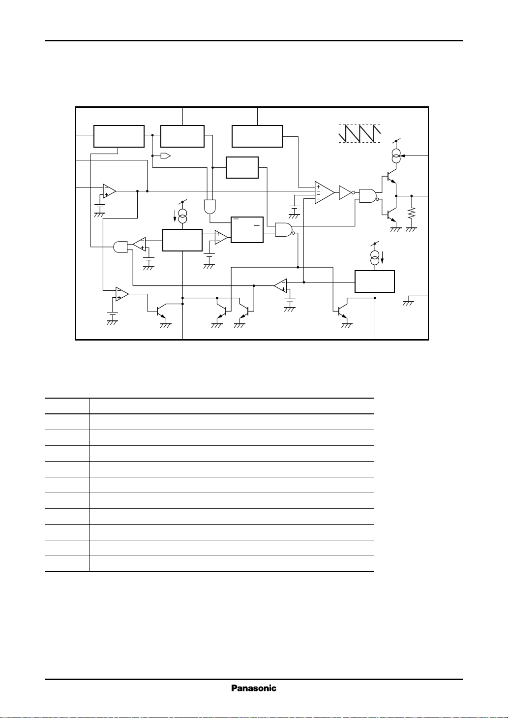
■ Block Diagram
CC
Off
FB
IN−
Active-high
4
10
Error amp.
1
Low level detector
comp.
1.27 V
On/off
control
1.27 V
S.C.P.
comp.
Reference
voltage supply
1.27 V
SS pin
V
CC
1 µA
Low level
clamp
0.23 V
V
5
U.V.L.O.
High level detector comp.
1.27 V
2
OSC
9
Triangular wave
generator
Latch
R
S
0.6 V
Q
Unlatch comp.
0.7 V
0.2 V
0.23 V
PWM
V
Low level
clamp
3
CC
5 µA
V
CC
30 kΩ
8
6
7
RB
Out
GND
S.C.P.
■ Pin Descriptions
Pin No. Symbol Description
1IN− Error amplifier inverting input
2 S.C.P. Time constant capacitor connection for short-circuit protection
3 SS Soft-start time-constant capacitor connection
4 Off On/off control
5VCCSupply voltage
6 Out Push-pull output
7 GND Ground
8 RB Output-current setting resistor connection pin
9 OSC Oscillator circuit timing resistor/capacitor connection pin
10 FB Error amplifier output
SS
3
Voltage Regulators AN8016NSH
■ Absolute Maximum Ratings
Parameter Symbol Rating Unit
Supply voltage V
Off pin allowable application voltage
IN− pin allowable application voltage
Out pin allowable application voltage
Supply current I
Output source current I
Output sink current I
Power dissipation
*
Operating temperature T
Storage temperature T
Note) 1. Currents or voltages may not be applied to any pins not stipulated above. For circuit currents, a positive (+) value indicates
current flowing into the IC, and a negative (−) value indicates current flowing out of the IC.
2. Items other than the storage temperature, operating temperature, and power dissipation are all stipulated at Ta = 25°C.
3. *: Ta = 85°C. For the independent IC without a heat sink. Note that the relationship between IC power dissipation and
the ambient temperature must follow the derating curve.
CC
V
OFF
V
IN−
V
OUT
CC
SO(OUT)
SI(OUT)
P
D
opr
stg
15 V
15 V
V
CC
V
15 V
mA
−50 mA
+50 mA
115 mW
−30 to +85 °C
−55 to +150 °C
■ Recommended Operating Range
Parameter Symbol Conditions Unit
Supply voltage V
Off control pin voltage V
Output source current I
Output sink current I
Timing resistance R
Timing capacitance C
Oscillator frequency f
Short-circuit protection time C
constant setting capacitance
Output current setting resistance R
CC
OFF
SO(OUT)
SI(OUT)
OUT
SCP
1.8 to 14 V
0 to 14 V
−40 (min.) mA
40 (max.) mA
T
T
3 to 30 kΩ
100 to 10 000 pF
20 to 1 000 kHz
1 000 (min.) pF
B
0 to 10k Ω
3
AN8016NSH Voltage Regulators
■ Electrical Characteristics at VCC = 2.4 V, Ta = 25°C
Parameter Symbol Conditions Min Typ Max Unit
U.V.L.O. block
Circuit operation start voltage V
UON
Error amplifier block
Input threshold voltage V
Line regulation with input fluctuation
V
Input bias current I
High-level output voltage V
Low-level output voltage V
PWM comparator block
Output source current I
Output block
Oscillator frequency f
OUT
Maximum duty Du
High-level output voltage V
Low-level output voltage V
Output source current I
Output sink current I
SO(OUT)VO
SI(OUT)VO
Pull-down resistor R
Unlatch circuit block
Input threshold voltage V
THUL
Short-circuit protection circuit block
Input threshold voltage V
Input standby voltage V
THPC
STBY
Input latch voltage V
Charge current I
CHG
On/off control block
Input threshold voltage V
Off mode SS pin voltage V
Off mode S.C.P. pin voltage V
ON(TH)
OFF(SS)
OFF(SCP)
Whole device
Average consumption current I
Latch mode consumption current I
Standby mode current I
CC(AV)
CC(LA)RB
CC(SB)
Voltage follower 1.23 1.27 1.31 V
TH
VCC = 1.8 V to 14 V 1.0 10 mV
dV
B
EH
EL
VSS = 0.5 V −3.5 −5 −6.5 µA
SS
RT = 12 kΩ, CT = 330 pF 170 190 2 10 kHz
max
IO = −15 mA, RB = 390 Ω 1.4 V
OH
IO = 10 mA, RB = 390 Ω0.2 V
OL
= 0.9 V, RB = 390 Ω−45 −32 −20 mA
= 0.3 V, RB = 390 Ω 20 mA
O
IN
V
= 0.5 V −1.65 −1.3 − 0.95 µA
SCP
RB = 390 Ω, Duty = 50% 3.4 5.0 mA
= 390 Ω1.8 2.4 mA
1.45 1.6 1.75 V
0.2 1.0 µA
1.85 2.0 2.15 V
0.2 V
75 80 85 %
20 30 40 kΩ
0.13 0.20 0.27 V
1.17 1.27 1.37 V
60 120 mV
40 120 mV
0.8 1.0 1.3 V
0.13 0.27 V
0.13 0.27 V
5 µA
5
Voltage Regulators AN8016NSH
■ Electrical Characteristics at VCC = 2.4 V, Ta = 25°C (continued)
•
Design reference data
Note) The characteristics listed below are theoretical values based on the IC design and are not guaranteed.
Parameter Symbol Conditions Min Typ Max Unit
U.V.L.O. block
Reset voltage V
Error amplifier block
VTH temperature characteristics V
Output source current I
Output sink current I
THdT
SO(FB)
SI(FB)
Open-loop gain A
PWM comparator block
SS pin voltage V
Output block
RB pin voltage V
Oscillator frequency supply f
voltage characteristics
Oscillator frequency temperature f
characteristics
Short-circuit protection circuit block
Comparator threshold voltage V
On/off control block
On/Off pin current I
OFF
R
Ta = −30°C to +85°C − 0.5 + 0.5 %
VFB = 0.5 V −40 µA
VFB = 0.5 V 2 mA
V
SS
RB = 390 Ω 0.13 V
B
VCC = 1.8 V to 14 V −1 +1%
dV
Ta = −30°C to 85°C −3 +3%
dT
THL
V
= 1.5 V 23 µA
OFF
0.8 V
80 dB
1.22 V
1.27 V
5
AN8016NSH Voltage Regulators
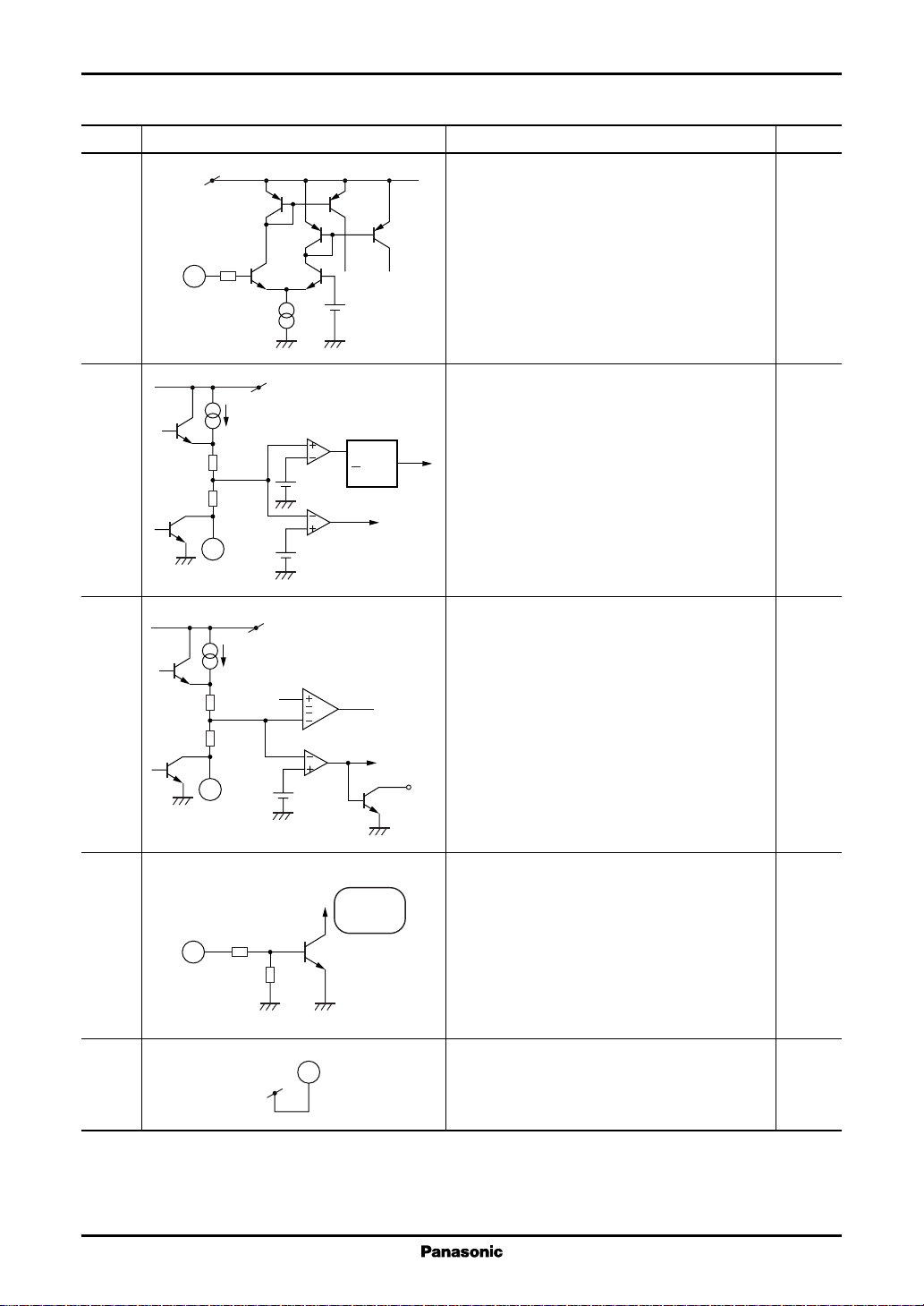
■ Terminal Equivalent Circuits
Pin No. Equivalent Circuit Description I/O
1IN−:I
V
CC
Error amplifier inverting input.
1
300 Ω
1.26 V
2 S.C.P.: O
2
0.23 V
3 kΩ
3 kΩ
V
CC
Latch
S
R
1.27 V
0.23 V
Low level detection comp.
Q
Output
cutoff
To the
on/off
control
circuit
Connection for the capacitor that sets the
timer latch short-circuit protection circuit time
constant. Use a capacitor with a value of
1 000 pF or higher.
The charge current I
is 1.3 µA (typical).
CHG
However, the capacitor is charged with a time
constant determined by 0.23 V and a resistance
of 6 kΩ until the pin voltage reaches 0.23 V.
3 SS: I
V
CC
Connection pin for the capacitor that determines
the PWM output soft start period. Note that the
0.23 V
3 kΩ
3 kΩ
3
PWM
C
T
Unlatch comp.
0.23 V
To the
on/off
control
circuit
S.C.P. pin
the short-circuit protection circuit does not
supply charge current to S.C.P. pin until this pin
voltage reaches about 0.2 V.
The source current I
is 5 µA (typical).
SS
However, the capacitor is charged with a time
constant determined by 0.23 V and a resistor of
6 kΩ until the pin voltage reaches 0.23 V.
4 Off: I
Internal
circuit
30 kΩ
start/stop
4
60 kΩ
This pin controls the on/off for the IC.
High-level input: normal operation
(V
> 1.3 V)
OFF
Low-level input: standby mode
(V
< 0.8 V)
OFF
In the standby state, the total IC current
consumption is decreased to 5 µA or under.
5
5
VCC:
Power supply connection.
Provide an operating supply voltage of 1.8 V
to 14 V.
7

Voltage Regulators AN8016NSH
■ Terminal Equivalent Circuits (continued)
Pin No. Equivalent Circuit Description I/O
6 Out: O
7 GND:
7
8 RB: I
V
CC
R1
8
I
O(SO)
V
CC
RB
30 kΩ
This is a push-pull output.
The absolute maximum rating for the output
current is ±50 mA. A constant-current output
with excellent line regulation and minimal
6
sample-to-sample variations can be acquired by
connected an external resistor to the RB pin.
IC ground.
Connection for the resistor that sets the output
current.
Use a resistor in the range 0 to 10 kΩ. Note that
the internal resistor R1 has a value of 1.0 kΩ.
Out
Thus the pin voltage will be 0.13 V when R
is
B
390 Ω.
9 OSC: O
10
V
CC
V
CC
Latch
S
Q
R
0.23 V
9
Connection for the capacitor and resistor that
determines the oscillator frequency. Use a
capacitor in the range 100 pF to 10 000 pF
and a resistor in the range 3 kΩ to 30 kΩ.
Use an oscillator frequency in the range
20 kHz to 1 MHz.
FB: O
Error amplifier output.
40 µA
C
PWM
A source current is about −40 µA and a sink
current is about 2 mA.
Correct the gain and the phase frequency
2 mA
characteristics by inserting a capacitor and
a resistor between this pin and IN− pin.
10
7

AN8016NSH Voltage Regulators
■ Usage Notes
•
Notes on IC power dissipation
Since the power dissipation in this IC increases proportionally with the supply voltage, applications must be careful
to operate so that the actual power dissipation does not exceed the power dissipation.
Since the output current set by the application circuit flows in the IC during the period corresponding to the output
on duty factor (Du, where Du
is 0.85), the IC power dissipation P is given by the following formula.
max
P = (V
CC
− V
BEQ1
) × I
× Du + VCC × ICC < P
OUT
D
■ Application Notes
[1] Power dissipation for the SSOP010-P-0225 package
PD T
a
400
386
Glass epoxy printed
300
287
(mW)
D
200
154
115
Power dissipation P
100
circuit board
(50 × 50 × t0.8 mm
= 259°C/W
R
th(j−a)
Independent IC
without a heat sink
R
= 348°C/W
th(j−a)
3
)
0
0 25 50 75 85 100 125 150
Ambient temperature Ta (°C)
9

Voltage Regulators AN8016NSH
■ Application Notes (continued)
[2] Main characteristics
Timing capacitance Oscillator frequency Maximum duty Oscillator frequency
1 000
RT = 3 kΩ
RT = 6.2 kΩ
100
Oscillator frequency (kHz)
10
RT = 12 kΩ
RT = 30 kΩ
100 1 000 10 000
Timing capacitance (pF)
95
90
85
RT = 12 kΩ
80
Maximum duty (%)
75
70
10 100 1 000
RT = 30 kΩ
RT = 3 kΩ
RT = 6.2 kΩ
Oscillator frequency (kHz)
Error amplifier VTH temperature characteristics Oscillator frequency temperature characteristics
1.28
1.278
1.276
192
190
188
186
Voltage (V)
1.274
1.272
−30 −10 90
10 30 50 70
Ambient temperature Ta (°C)
Maximum duty temperature characteristics
81
80
79
78
Maximum duty (%)
77
76
−30 −10 90
10 30 50 70
Ambient temperature Ta (°C)
184
Oscillator frequency (kHz)
182
180
−30 −10 90
10 30 50 70
Ambient temperature Ta (°C)
9

AN8016NSH Voltage Regulators
■ Application Notes (continued)
[3] Timing charts (internal waveforms)
High
Off pin voltage
Power on
Supply voltage (V
Triangular wave (CT)
CC
)
Error amplifier output (FB)
S.C.P. pin voltage
SS pin voltage
Low
2.4 V
2.0 V
1.27 V
1.22 V
0.7 V
0.6 V
0.4 V
0.2 V
High
Out pin waveform
Short-circuit protection
comparator threshold level
Dead time voltage (VDT)
Error amplifier output (FB)
Triangular wave (CT)
Out pin waveform
S.C.P. pin voltage
Short-circuit protection
comparator output
Soft start operation
Figure 1. PWM comparator operating waveforms
Maximum duty: 80%
Low
2.0 V
1.27 V
0.6 V
High
Low
1.27 V
0.06 V
t
PE
High
Low
11
Figure 2. Short-circuit protection operating waveforms

Voltage Regulators AN8016NSH
■ Application Notes (continued)
[4] Functional descriptions
1. Reference voltage block
This circuit is composed of a band gap circuit, and outputs a 1.26-volt temperature compensated reference
voltage. This reference voltage is stabilized when the supply voltage is 1.8 V or higher.
2. Triangular wave generator
This circuit generates a triangular wave like
sawtooth with a peak of 0.75 V and a trough of 0.2
V using a capacitor (for the time constant) and resistor connected to the OSC pin (pin 9). The oscillator
frequency can be set to any value by selecting appropriate values for the external capacitor and resistor,
C
and RT. This oscillator can provide a frequency in
T
the range 20 kHz to 1 MHz. The triangular wave signal is provided to the inverting input of the PWM
comparator internally to the IC. Use the formulas
below for rough calculation of the oscillator frequency.
t
1
t
2
DischargeRapid
charge
T
Figure 1. Triangular oscillator waveform
V
V
OSCH
OSCL
≈ 0.75 V
≈ 0.2 V
f
OSC
≈ −
1
CT × RT × ln
V
V
≈ 0.75 ×
OSCL
OSCH
1
CT × R
[Hz]
T
Note, however, that the above formulas do not take the rapid charge time, overshoot, and undershoot into
account. See the experimentally determined graph of the oscillator frequency vs. timing capacitance value
provided in the main characteristics section.
3. Error amplifier
This circuit is an npn-transistor input error ampli-
fier that detects and amplifies the DC-DC converter
output voltage, and inputs that signal to a PWM comparator. The 1.27 V internal reference voltage is
applied to the noninverting input. Arbitrary gain and
phase compensation can be set up by inserting a resistor and capacitor in series between the error amplifier output pin (pin 10) and the inverting input pin
(pin 1). The output voltage V
can be set by resis-
OUT
tor-dividing the output as shown in figure 2.
R1
R2
V
OUT
V
OUT
FB
IN− 1
= 1.27 ×
10
R1 + R2
Error
amplifier
1.27 V
R2
To the PWM
comparator input
Figure 2. Connection method of error amplifier
11

AN8016NSH Voltage Regulators
■ Application Notes (continued)
[4] Function descriptions (continued)
4. Timer latch short-circuit protection circuit
This circuit protects the external main switching element, flywheel diode, choke coil, and other components
against degradation or destruction if an excessive load or a short circuit of the power supply output continues
for longer than a certain fixed period.
The timer latch short-circuit protection circuit detects the output of the error amplifiers. If the DC-DC
converter output voltage drops and an error amplifier output level exceeds 1.27 V, this circuit outputs a low level
and the timer circuit starts. This starts charging the external protection circuit delay time capacitor.
If the error amplifier output does not return to the normal voltage range before that capacitor reaches 1.27
V, the latch circuit latches, the output drive transistors are turned off, and the off-period is set to 100%.
5. Low input voltage malfunction prevention circuit (U.V.L.O.)
This circuit protects the system against degradation or destruction due to incorrect control operation when
the power supply voltage falls during power on or power off.
The low input voltage malfunction prevention circuit detects the internal reference voltage that changes with
the supply voltage level. While the supply voltage is rising, this circuit cuts off the output drive transistor until
the reference voltage reaches 1.6 V. It also sets the off-period to 100%, and at the same time holds the S.C.P. pin
(pin 2) and the SS pin (pin 3) at the low level.
6. PWM comparator
The PWM comparator controls the on-period of the output pulse according to its input voltage. The output
transistors are turned on during periods when the OSC pin (pin 9) triangular waveform is lower than the error
amplifier output pin (pin 10), the SS pin (pin 3), and the IC internally fixed dead-time voltage (about 0.6 V).
The maximum duty is fixed at 80% (typical).
The SS pin provides a constant-current source output of 5 µA (typical), and can be used to implement soft
start operation in which the output pulse on period is gradually increased by connecting an external capacitor to
that pin. Note that the SS pin charge operation completes when the SS pin voltage reaches 1.22 V (typical).
7. Unlatch block
The unlatch circuit holds the S.C.P. fixed at the low level while the SS pin voltage reaches the soft start
operation start-level (about 0.23 V) when power is first applied. This suppresses increases in the short-circuit
protection detection time associated with longer startup times.
8. Output block
The output circuit has a totem pole structure. A constant-current source output with good line regulation can
be set up at an arbitrary voltage by connecting a current setting resistor to the RB pin.
This circuit can provide an output current of up to 50 mA. The output pin has a breakdown voltage of 15 V.
9. On/off control block
The IC can be turned on or off externally. When the Off pin (pin 4) voltage is set by the application of about
1.3 V or higher, the internal reference voltage is turned on, and control operation starts. If the Off pin voltage is
dropped to about 0.8 V or lower, after the S.C.P. pin and SS pin external capacitors discharge, the internal
reference voltage is turned off and IC control operation is stopped. This reduces IC current consumption to 5 µA
or under.
13

Voltage Regulators AN8016NSH
■ Application Notes (continued)
[5] Time constant setup for the timer latch short-circuit protection circuit
Figure 4 shows the structure of the timer latch short-circuit protection circuit. The short-circuit protection
comparator continuously compares a 1.27 V reference voltage with the error amplifier output V
When the DC-DC converter output load conditions are stable, the short-circuit protection comparator holds its
average value, since there are no fluctuations in the error amplifier outputs. At this time, the output transistor Q1
will be in the conducting state, and the S.C.P. pin will be held at about 60 mV.
If the output load conditions change rapidly and a high-level signal (1.27 V or higher) is input to the shortcircuit protection comparator's non-inverting input from the error amplifier, the short-circuit protection comparator
will output a low level and the output transistor Q1 will shut off. Then, the external capacitor C
S.C.P. pin will start to charge. When the external capacitor C
is charged to about 1.27 V, the latch circuit will latch
S
and the off-period will be set to 100% with the output held fixed at the low level. Once the latch circuit has latched,
the S.C.P. pin capacitor will be discharged to about 40 mV, but the latch circuit will not reset unless either power
is turned off or the power supply is restarted using on/off control.
The capacitor C
is charged from 60 mV to about 230 mV with a time constant determined by a resistor of 6 kΩ,
S
and is charged from 230 mV to 1.26 V by a constant current of about 1.3 µA.
.
FB
connected to the
S
1) 0.06 ≤ V
V
t
PE1
2) 0.23 ≤ V
SCP
= (0.23 − 0.06) × {1 − exp( −
SCP
[s] ≈ 0.017 × CS [mF]
SCP
1.27 V = 0.23 V + I
t
[s] ≈ 0.80 × CS [µF]
PE2
[s] ≈ t
∴ t
PE
FB 10
IN− 1
[V] ≤ 0.23
[V] ≤ 1.26
CHG
+ t
PE1
PE2
Error amp.
1.27 V
t
PE1
6k · C
t
PE2
×
C
S
≈ 0.817 × CS [µF]
On/off
control
1.27 V
V
CC
S.C.P. comp.
3 kΩ
3 kΩ
Q1
V
)} [V]
S
1 µA
0.23 V
High level detection comparator
1.27 V
SCP
1.27
0.23
0.06
t
PE1
Figure 3. S.C.P. pin charging waveform
U.V.L.O.
Latch
R
S
[V]
Short-circuit detection time t
t
PE2
Internal reference
Output
shutoff
Q
PE
t [s]
C
S.C.P. 2
S
Figure 4. Short-circuit protection circuit
At power supply startup, the output appears to be in the shorted state, the error amplifier output goes to the high
level, and the IC starts to charge the S.C.P. pin capacitor. Therefore, users must select an external capacitor that allows
the DC-DC converter output voltage to rise before the latch circuit in the later stage latches. In particular, care is
required if the soft start function is used, since that function makes the startup time longer.
13

AN8016NSH Voltage Regulators
■ Application Notes (continued)
[6] Setting the soft start time
A soft start function, which gradually increases the width of the output pulses at power on, will be applied if a
capacitor is connected to the SS pin. This can prevent rush currents and overshoot when the power supply is turned
on.
The capacitor C
kΩ, and is charged from 230 mV to 1.22 V by a constant current of about 5 µA.
The following formulas express the soft start time for the duty of up to 50%.
is charged from 60 mV to about 230 mV with a time constant determined by a resistor of 6
SS
1) 0.06 ≤ V
V
t
PE1
2) 0.23 ≤ V
SCP
= (0.23 − 0.06) × {1 − exp( −
SCP
[s] ≈ 0.017 × CS [mF]
SCP
0.52 V = 0.23 V + I
t
[s] ≈ 0.058 × CS [µF]
PE2
[s] ≈ t
∴ t
SS
[V] ≤ 0.23
[V] ≤ 1.26
CHG
+ t
SS1
≈ 0.075 × CS [µF]
SS2
(V)
1.22
0.75
0.52
0.23
0.06
t
SS1
×
FB
OSC
t
SS1
)} [V]
6k · C
S
t
SS2
C
S
SS
t
SS2
Duty: 50%
t (s)
15
Soft start time
DC-DC converter output voltage
Figure 5. Soft start operating waveforms

Voltage Regulators AN8016NSH
■ Application Notes (continued)
[7] Parallel synchronous operation of multiple ICs
Multiple instances of this IC can be operated in parallel. All the ICs will operate at the same frequency if the master
and slave IC OSC pins (pin 9) are connected directly.
1. Notes on S.C.P. operation during parallel operation
In the circuit in figure 6, if either the IC operating in master mode or the IC in slave mode detects a short circuit,
the IC that detected the short circuit will enter latched mode. The latched mode state is a state in which the
output is shut off and both the RB pin and the SS pin are set to the low level. However in this mode, this IC has
an added function that holds the OSC pin at the high level (about 0.8 V).
When OSC pin of the IC that did not enter latched mode goes to the high level, the internally fixed dead- time
voltage (about 0.6 V) will then be lower than the OSC pin voltage, and internal PWM circuit output will stop.
That will cause this IC to go to the output shorted state, and then, this IC will also switch to latched mode.
Therefore, applications that require parallel synchronous operation should adopt the basic circuit structure
shown in figure 6.
2. Usage notes
1) If capacitors are shared as shown in figure 7 to reduce the number of external components:
• The charge current will be doubled.
• The short-circuit protection circuit will not operate if the S.C.P. pin capacitor is shared.
In this circuit, even if the master IC detects a short circuit, the slave IC will not detect that state, so the
S.C.P. pin will remain fixed at the low level state. Note that as a result, the short-circuit protection circuit
will not operate and the IC will continue to operate at the maximum duty drive.
OSC
65
74
83
92
101
AN8016NSH Master
S.C.P.
Figure 6. Slave operation circuit example
2) Note that it is not possible to operate this IC (the AN8016NSH) with the two-channel AN8017SA/AN8018SA
together in parallel synchronous mode.
SS
92
101
AN8016NSH Slave
65
74
83
SSS.C.P.
OSC
65
74
83
92
101
AN8016NSH Master
S.C.P.
NG
Figure 7. Slave operation circuit example
92
101
AN8016NSH Slave
65
74
83
SS
15

AN8016NSH Voltage Regulators
■ Application Circuit Examples
[1] Application circuit (Step-up circuit)
330 pF
12 kΩ
390 Ω
0.1 µF
1 kΩ
FB10IN− 1
OSC9S.C.P. 2
RB8SS 3
AN8016NSH
333 pF
103 pF
6.8 kΩ
20 kΩ
GND7Off 4
1.5 V
V
3 V
Out6V
5
CC
IN
1 µF
47 µH
MA2Q738 (MA738∗)
2SD2408
Note) ∗: Former part number
Q1
SBD
10 µF
V
OUT
5 V
200 mA
The figure shows a step-up circuit that converts a 3 V input to a 5 V output.
The AN8016NSH output stage has a totem pole circuit configuration, and can directly drive an n-channel
MOSFET while minimizes switching loss and increasing efficiency. In this case, replace the npn transistor with an
n-channel MOSFET in above circuit.
[2] Notes on direct n-channel MOSFET drive
1. Select an n-channel MOSFET with a low input
capacitance.
The AN8016NSH was designed to drive bipolar
transistors, and adopts a circuit structure that can provide a constant-current (50 mA maximum) output
source current. Furthermore, it has a sink current capacity of about 50 mA. This means that designs must
be concerned about increased power dissipation due
to increased rise and fall times. If problems occur, an
inverter may be inserted as shown in figure 1 to provide amplification.
2. Use an n-channel MOSFET of a low gate threshold
voltage.
Since the AN8016NSH Out pin high-level output
voltage is V
− 1.0 V (minimum), a low VT MOSFET
CC
with an adequately low on-resistance must be used.
Also, if a large V
is required, one solution is to use
GS
a transformer as shown in figure 2, and apply a voltage of twice the input voltage to the IC's V
CC
pin.
V
IN
6
Out
Figure 1. Output boosting circuit
V
IN
V
CC
SBD
5
6
Out
VCC ≈ 2 × VIN − V
Figure 2. Gate drive voltage boosting technique
SBD
SBD
V
OUT
V
OUT
D
17

Voltage Regulators AN8016NSH
■ Application Circuit Examples (continued)
[2] Notes on direct n-channel MOSFET drive (continued)
3. Notes on printed circuit board pattern layout
Observe the following recommendations on printed circuit board pattern layout to achieve low noise and high
efficiency.
1) Use extremely wide lines for the ground lines, and isolate the IC ground from the power system ground.
2) Make the lines in the high-current system as wide as possible.
3) Position the input filter capacitor C3 as close as possible to the V
are no other paths for switching noise to enter the IC.
4) Keep the length of the line between the Out pin and the switching device (either a MOSFET or other
transistor) as short as possible to provide a clean switching waveform to the switching device.
5) Use a relatively long line for the low-impedance side of the output voltage detection resistor R2.
V
IN
RB8
FB10IN− 1
OSC9
GND7
Out6V
and ground pins, and assure that there
CC
(2)
SBD
Q1
(4)
V
OUT
GND
(1)
[3] Evaluation board
AN8016NSH
S.C.P. 2
24
kΩ
R2
SS 3
Off V
5
CC
Off 4
C3
IN
L1
C3
C1C2
R1
AN8016NSH
R2
DC-DC CONVERTER BOARD
R4
R3
(3)
+
SBD
Q1
BCE
C4
R5
(5)
V
OUT
+
C6
GND
R6
C5
17
 Loading...