

Panasonic AN79M09F, AN79M09, AN79M08F, AN79M08, AN79M07F Datasheet
...
AN79M00/AN79M00F Series
3-pin Negative Output Voltage Regulators (500mA Type)
■ Overview
The AN79M00 and the AN79M00F series are 3-pin
fixed ne gative output voltage regulators. Stabilized fixed
output voltage is obtained from unstable DC input voltage without using any external components. 12 types of
output voltage are available ; –5V, –5.2V, –6V, –7V, –8V ,
–9V, –10V, –12V, –15V, –18V, –20V and –24V. They can
be used widely in power circuits with current capacitance
up to 500mA.
■ Features
• No external components
• Output voltage : –5V, –5.2V, –6V, –7V, –8V, –9V, –10V,
–12V, –15V, –18V, –20V, –24V
• Short-circuit current limiting built-in
• Thermal overload protection built-in
• Output transistor safe area compensation
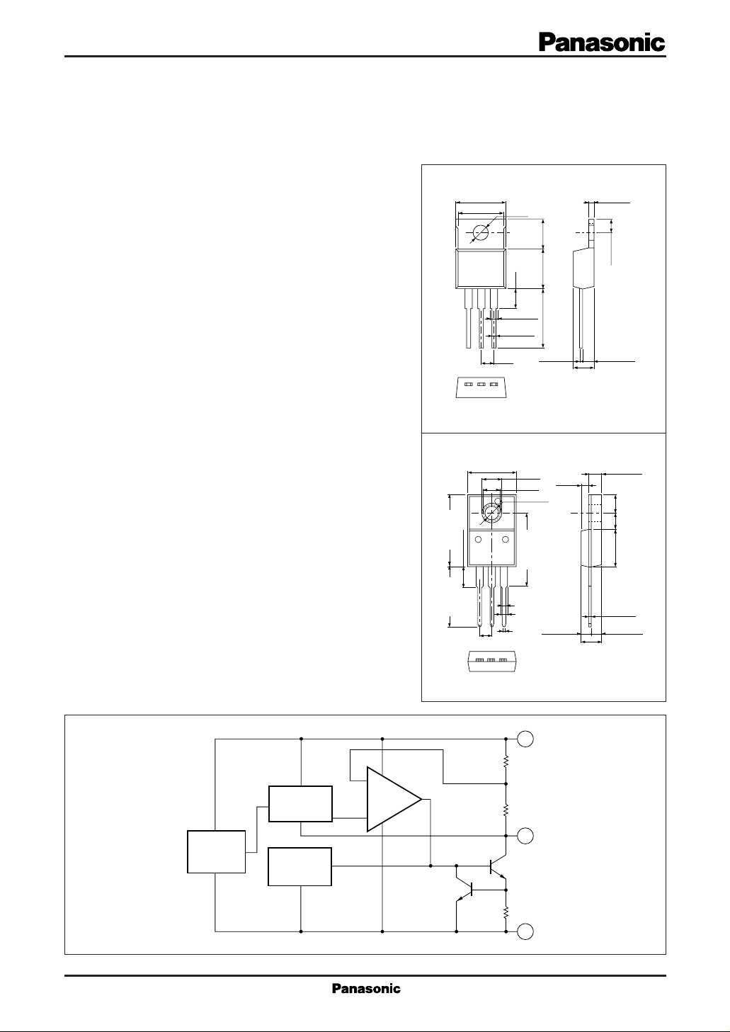
AN79M00 Series
10.5±0.5
10.4±0.5
123
JEDEC:TO-220AB. (HSIP003-P-0000)
AN79M00F Series
10.5±0.3
16.7±0.3
4.5±0.25
ø3.7
1.4±0.25
0.8±0.2
2.54
4.5
ø5.3
(4.3)
3.1±0.1
17.0±0.25
0.45
6.7±0.258.7±0.313.6±0.25
+0.1
– 0.05
(1.73)
4.5±0.3
1.4±0.1
2.9±0.1
2.5±0.25
1 : Common
2 : Input
3 : Output
2.77±0.3
Unit:mm
Unit:mm
4.2±0.25
3.8±0.25
8.7±0.3
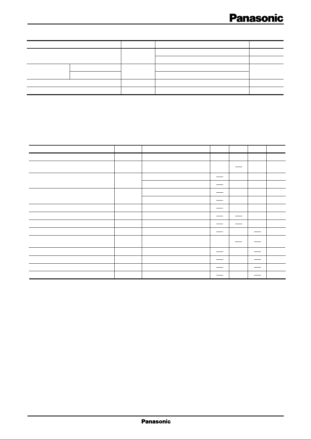
■ Block Diagram
Starter
Voltage
Reference
Thermal
Protection
+
Error Amp.
–
Current
Limiter
2.54
123
R
1
R
2
Q
1
R
SC
0.8±0.2
1.4±0.2
(0.4)
1
3
Pass Tr.
2
4.5±0.3
Common
Output
Input
13.6±0.25
TO-220 Full Pack Package (HSIP003-P-0000A)
+0.1
0.4
– 0.05
2.5±0.252.0±0.25
1 : Common
2 : Input
3 : Output
■ Absolute Maximum Ratings (Ta=25˚C)
Parameter Symbol Rating Unit
1
*
Input voltage
Power dissipation
AN79M00 Series
AN79M00F Series
Operating ambient temperature
Storage temperature
*
1 AN79M05/F, AN79M52/F, AN79M06/F, AN79M07/F, AN79M08/F, AN79M09/F, AN79M10/F, AN79M12/F,
V
I
P
D
T
opr
T
stg
–35
2
*
–40
3
*
15
3
*
10.25
–20 to +80
–55 to +150
AN79M15/F, AN79M18/F
*
2 AN79M20/F, AN79M24/F
*
3 Follow the derating curve. When T
exceeds 150˚C, the internal circuit cuts off the output.
j
■ Electrical Characteristics (Ta=25˚C)
AN79M05/AN79M05F (–5V Type)
·
Parameter Symbol Condition min typ max
Output voltage
Output voltage tolerance
Line regulation
Load regulation
Bias current
Input bias current fluctuation
Load bias current fluctuation
Output noise voltage
Ripple rejection ratio
Minimum input/output voltage difference
Output short circuit current
Peak output current
Output voltage temperature coefficient
Note 1) The specified condition T
=25˚C means that the test should be carried out with the test time so short (within 10ms) that the
j
drift in characteristic value due to the rise in chip junction temperature can be ignored.
Note 2) When not specified, V
*
AN79M05 : 15W, AN79M05F : 10.25W
=–10V, IO=350mA, CI=2µF, CO=1µF and Tj=0 to 125˚C
I
REG
REG
∆I
∆I
V
DIF (min.)
I
I
V
O
V
O
I
Bias
bias (IN)
bias (L)
V
no
RR
O (Short)
O (peak)
T
=25˚C
j
=–7 to –25V,
V
I
=5 to 350mA, P
I
O
=–7 to –25V, Tj=25˚C
V
I
IN
=–8 to –18V, Tj=25˚C
V
I
=5 to 500mA, Tj=25˚C
I
O
L
=5 to 350mA, Tj=25˚C
I
O
=25˚C
T
j
=–8 to –25V, Tj=25˚C
V
I
=5 to 350mA, Tj=25˚C
I
O
f=10Hz to 100kHz, Ta=25˚C
=–8 to –18V, IO=100mA,
V
I
f=120Hz, Ta=25˚C
T
=25˚C
j
=–35V, Tj=25˚C
V
I
Tj=25˚C
=5mA, Tj=0 to 125˚C
I
O
D
–4.8
<
*
=
–4.75
1
10
125
60
– 0.4∆VO/Ta
–5.2 V–5
–5.25
50 mV3
30
100
50
0.8
0.4
4
V
V
W
˚C
˚C
Unit
V
mV
mV20
mV
mA2
mA
mA
µV
dB
V1.1
mA50
mA1000
mV/˚C
■ Electrical Characteristics (Ta=25˚C)
AN79M52/AN79M52F (–5.2V Type)
·
Parameter Symbol Condition min typ max
Output voltage
Output voltage tolerance
Line regulation
Load regulation
Bias current
Input bias current fluctuation
Load bias current fluctuation
V
V
REG
REG
Bias
∆I
bias (IN)
∆I
bias (L)
Output noise voltage
Ripple rejection ratio
Minimum input/output voltage difference
Output short circuit current
Peak output current
Output voltage temperature coefficient
Note 1) The specified condition T
=25˚C means that the test should be carried out with the test time so short (within 10ms) that the
j
RR
V
DIF (min.)
I
O (Short)
I
O (peak)
∆V
drift in characteristic value due to the rise in chip junction temperature can be ignored.
Note 2) When not specified, VI=–10V, IO=350mA, CI=2µF, CO=1µF and Tj=0 to 125˚C
*
AN79M52 : 15W, AN79M52F : 10.25W
T
=25˚C
O
O
j
VI=–7 to –25V,
=5 to 350mA, P
I
O
V
=–7 to –25V, Tj=25˚C
I
IN
=–8 to –18V, Tj=25˚C
V
I
I
=5 to 500mA, Tj=25˚C
O
L
IO=5 to 350mA, Tj=25˚C
T
=25˚C
j
VI=–8 to –25V, Tj=25˚C
IO=5 to 350mA, Tj=25˚C
f=10Hz to 100kHz, Ta=25˚C
no
=–8 to –18V, f=120Hz,
V
I
=100mA
I
O
T
=25˚C
j
VI=–35V, Tj=25˚C
Tj=25˚C
=5mA, Tj=0 to 125˚C
I
/Ta
O
O
D
<
*
=
–5.0
–4.94
60
130V
– 0.4
–5.4 V–5.2
–5.46
50 mV
30
100
50
4
0.8
0.4
Unit
V
mV
mV
mV
mA2I
mA
mA
µV
dB
V1.1
mA50
mA1000
mV/˚C
AN79M06/AN79M06F (–6V Type)
·
Parameter Symbol Condition min typ max
Output voltage
Output voltage tolerance
Line regulation
Load regulation
Bias current
Input bias current fluctuation
Load bias current fluctuation
Output noise voltage
Ripple rejection ratio
Minimum input/output voltage difference
Output short circuit current
Peak output current
Output voltage temperature coefficient
Note 1) The specified condition T
=25˚C means that the test should be carried out with the test time so short (within 10ms) that the
j
REG
REG
∆I
∆I
V
DIF (min.)
I
O (Short)
I
O (peak)
DV
V
O
V
O
Bias
bias (IN)
bias (L)
no
RR
/Ta
O
=25˚C
T
j
V
=–8 to –25V,
I
=3 to 350mA, P
I
O
V
=–8 to –25V, Tj=25˚C
I
IN
=–9 to –19V, Tj=25˚C
V
I
I
=5 to 500mA, Tj=25˚C
O
L
IO=5 to 350mA, Tj=25˚C
T
=25˚C
j
VI=–9 to –25V, Tj=25˚C
IO=5 to 350mA, Tj=25˚C
f=10Hz to 100kHz, Ta=25˚C
=–9 to –19V, IO=100mA,
V
I
f=120Hz, Ta=25˚C
=25˚C
T
j
VI=–35V, Tj=25˚C
Tj=25˚C
=5mA, Tj=0 to 125˚C
I
O
D
<
*
=
drift in characteristic value due to the rise in chip junction temperature can be ignored.
Note 2) When not specified, VI=–11V, IO=350mA, CI=2µF, CO=1µF and Tj=0 to 125˚C
*
AN79M06 : 15W, AN79M06F : 10.25W
–5.75
–5.7
60
1.5
20
10
150V
–0.4
5
–6.25 V–6
–6.3
60 mV
40
120
60
4
0.8
0.4
Unit
V
mV
mV
mV
mA2I
mA
mA
µV
dB
V1.1
mA50
mA1000
mV/˚C
 Loading...