

Panasonic AN7809, AN7808F, AN7808, AN7807F, AN7807 Datasheet
...
AN7800/AN7800F Series
3-pin Positive Output Voltage Regulator (1A Type)
■ Overview
The AN7800 series and the AN7800F series are 3-pin
fixed positive output voltage regulators. Stabilized fixed
output voltage is obtained from unstable DC input voltage without using external components. 11 types of fixed
output voltage are available, 5V, 6V, 7V, 8V, 9V, 10V,
12V, 15V , 18V, 20V and 24V. They can be used widely in
power circuits with current capacity up to 1A.
■ Features
• No external components
• Output voltage:5V, 6V, 7V, 8V, 9V, 10V,
12V, 15V, 18V, 20V, 24V
• Internal short-circuit current limiting
• Internal thermal overload protection
• Output transistor safe area compensation
10.5±0.5
10.4±0.5
16.7±0.3
ø3.7
6.7±0.258.7±0.313.6±0.25
4.5
1.4±0.25
0.8±0.2
2.54
0.45
123
JEDEC:TO-220AB (HSIP003-P-0000)
10.5±0.3
ø5.3
(4.3)
3.1±0.1
4.5±0.25
17.0±0.25
+0.1
– 0.05
4.5±0.3
(1.73)
1.4±0.1
2.9±0.1
2.5±0.25
1:Input
2:Common
3:Output
Unit:mmAN7800 Series
Unit:mmAN7800F Series
2.77±0.3
4.2±0.25
3.8±0.25
8.7±0.3
■ Block Diagram
Starter
Voltage
Reference
Current
Source
+
ErrorAmp.
–
13.6±0.25
TO-220 Full Pack Package (HSIP003-P-0000A)
Pass Tr
Current
Limiter
Thermal
Protection
2.54
123
(0.4)
0.8±0.2
1.4±0.2
Q
1
R
SC
R
2
R
1
1
3
2
Input
Output
Common
4.5±0.3
+0.1
0.4
– 0.05
2.5±0.252.0±0.25
1:Input
2:Common
3:Output
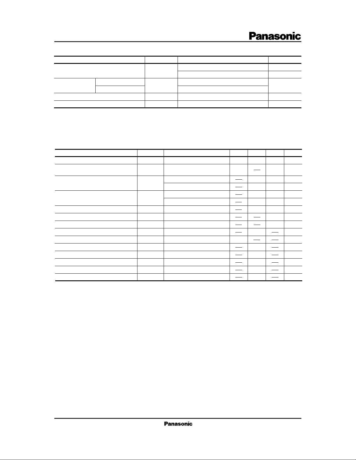
■ Absolute Maximum Ratings (Ta=25˚C)
Parameter Symbol Rating Unit
1
*
Input voltage
Power dissipation
AN7800 Series
AN7800F Series
Operating ambient temperature
Storage temperature
*
1 AN7805/F, AN7806/F, AN7807/F, AN7808/F, AN7809/F, AN7810/F, AN7812/F, AN7815/F, AN7818/F
*
2 AN7820/F, AN7824/F
*
3 Follow the derating curve. When T
exceeds 150˚C, the internal circuit cuts off output.
j
V
I
P
D
T
opr
T
stg
35
2
*
40
3
*
15
*
10.25
–30 to+80
–55 to+150
3
■ Electrical Characteristics (Ta=25˚C)
AN7805/7805F (5V Type)
·
Parameter Symbol Condition min typ max Unit
Output voltage
Output voltage tolerance
Line regulation
Load regulation
Bias current
Input bias current change
Load bias current change
Output noise voltage
Ripple rejection ratio
Minimum input/output voltage difference
Output impedance
Output short circuit current
Peak output current
REG
REG
∆I
V
DIF (min.)
I
O (Short)
I
O (Peak)
V
O
V
O
I
bias
bias (IN)
bias (L)
V
no
RR
O
Output voltage temperature coefficient
Note 1) The specified condition T
=25˚C means that the test should be carried out with the test time so short (within 10ms) that the
j
drift in characteristic value due to the rise in chip junction temperature can be ignored.
Note 2) When not specified, VI=10V, IO=500mA, CI=0.33µF and CO=0.1µF.
*
AN7800 Series:15W, AN7800F Series:10.25W
=25˚C
T
j
=8 to 20V, IO=5mA to 1A,
V
I
=0 to 125˚C, P
T
j
=7.5 to 25V, Tj=25˚C
V
I
IN
=8 to 12V, Tj=25˚C
V
I
=5mA to 1.5A, Tj=25˚C
I
O
L
=250 to 750mA, Tj=25˚C
I
O
=25˚C
T
j
=7.5 to 25V, Tj=25˚C
V
I
=5mA to 1A, Tj=25˚C
I
O
f=10Hz to 100kHz
VI=8 to 18V, IO=100mA, f=120Hz
=1A, Tj=25˚C
I
O
f=1kHz
=25V, Tj=25˚C
V
I
Tj=25˚C
=5mA, Tj=0 to 125˚C
I
O
D
<
*
=
4.8
4.75
62
V
V
W
˚C
˚C
5.2 V5
5.25
V
100 mV3
50
50
1.3
0.5
mV
mV15
mV
mA3.9
8
mA
mA∆I
1
100
5
µV40
dB
V2
mΩ17Z
mA700
A2
mV/˚C– 0.3∆VO/Ta
■ Electrical Characteristics (Ta=25˚C)
AN7806/7806F (6V Type)
·
Parameter Symbol Condition min typ max Unit
Output voltage
Output voltage tolerance
Line regulation
Load regulation
Bias current
Input bias current change
Load bias current change
Output noise voltage
Ripple rejection ratio
Minimum input/output voltage difference
REG
REG
∆I
∆I
V
DIF (min.)
V
V
I
bias
bias (IN)
bias (L)
V
RR
Output impedance
Output short circuit current
Peak output current
I
O (Short)
I
O (Peak)
Output voltage temperature coefficient
Note 1) The specified condition T
=25˚C means that the test should be carried out with the test time so short (within 10ms) that the
j
drift in characteristic value due to the rise in chip junction temperature can be ignored.
Note 2) When not specified, VI=11V, IO=500mA, CI=0.33µF and CO=0.1µF.
*
AN7800 Series:15W, AN7800F Series:10.25W
T
=25˚C
O
O
no
j
=9 to 21V, IO=5mA to 1A,
V
I
=0 to 125˚C, P
T
j
=8.5 to 25V, Tj=25˚C
V
I
IN
=9 to 13V, Tj=25˚C
V
I
=5mA to 1.5A, Tj=25˚C
I
O
L
=250 to 750mA, Tj=25˚C
I
O
=25˚C
T
j
=8.5 to 25V, Tj=25˚C
V
I
=5mA to 1A, Tj=25˚C
I
O
f=10Hz to 100kHz
VI=9 to 19V, IO=100mA, f=120Hz
=1A, Tj=25˚C
I
O
f=1kHz
O
=25V, Tj=25˚C
V
I
Tj=25˚C
IO=5mA, Tj=0 to 125˚C
D
<
*
=
5.75
5.7
59
1.5
– 0.4
6.25 V6
6.3
V
120 mV5
mV
60
60
1.3
0.5
mV14
mV
mA3.9
8
mA
mA
µV
120
4
40
dB
V2
17Z
mΩ
mA700
A2
mV/˚C∆VO/Ta
AN7807/7807F (7V Type)
·
Parameter Symbol Condition min typ max Unit
Output voltage
Output voltage tolerance
Line regulation
Load regulation
Bias current
Input bias current change
Load bias current change
Output noise voltage
Ripple rejection ratio
Minimum input/output voltage difference
Output impedance
Output short circuit current
Peak output current
Output voltage temperature coefficient
Note 1) The specified condition T
=25˚C means that the test should be carried out with the test time so short (within 10ms) that the
j
REG
REG
∆I
∆I
V
DIF (min.)
I
O (Short)
I
O (Peak)
V
O
V
O
I
bias
bias (IN)
bias (L)
V
no
RR
O
=25˚C
T
j
=10 to 22V, IO=5mA to 1A,
V
I
=0 to 125˚C, P
T
j
=9.5 to 25V, Tj=25˚C
V
I
IN
=10 to 15V, Tj=25˚C
V
I
=5mA to 1.5A, Tj=25˚C
I
O
L
=250 to 750mA, Tj=25˚C
I
O
=25˚C
T
j
=9.5 to 25V, Tj=25˚C
V
I
=5mA to 1A, Tj=25˚C
I
O
f=10Hz to 100kHz
VI=10 to 20V, IO=100mA, f=120Hz
=1A, Tj=25˚C
I
O
f=1kHz
=25V, Tj=25˚C
V
I
Tj=25˚C
IO=5mA, Tj=0 to 125˚C
D
<
*
=
drift in characteristic value due to the rise in chip junction temperature can be ignored.
Note 2) When not specified, VI=12V, IO=500mA, CI=0.33µF and CO=0.1µF.
*
AN7800 Series:15W, AN7800F Series:10.25W
6.7
6.6
7.3 V7
7.4
V
140 mV5
1.5
140
4
46
57
70
70
0.5
mV
mV14
mV
mA3.9
8
mA
1
mA
µV
dB
V2
16Z
mΩ
mA700
A2
– 0.5
mV/˚C∆VO/Ta
 Loading...