

Panasonic AN7176K, AN7171NK, AN7171K Datasheet
ICs for Audio Common Use
■ Overview
The AN7171NK and AN7176K are ICs for power amplification of 14W (13.2V, 4Ω) output. It can provide stereo
operation since two BTL amplifiers are incorporated in a
chip. It incorporates various protective circuits, thus providing high reliability. The circuits can be turned on or off
with supply pins energized, because the stand-by circuit
is built-in.
■ Features
•
Two BTL 14W outputs built-in
•
Stand-by circuit built-in
•
Various protective circuits (for temperature, or against
over-voltage, short-circuit between output and earth
and between output and VCC, load short-circuit)
•
Small shock noise at power ON/OFF
•
Fewer external components required
•
Good oscillation stability
AN7171NK, AN7176K
Dual BTL 14W Audio Power Amplifier Circuits
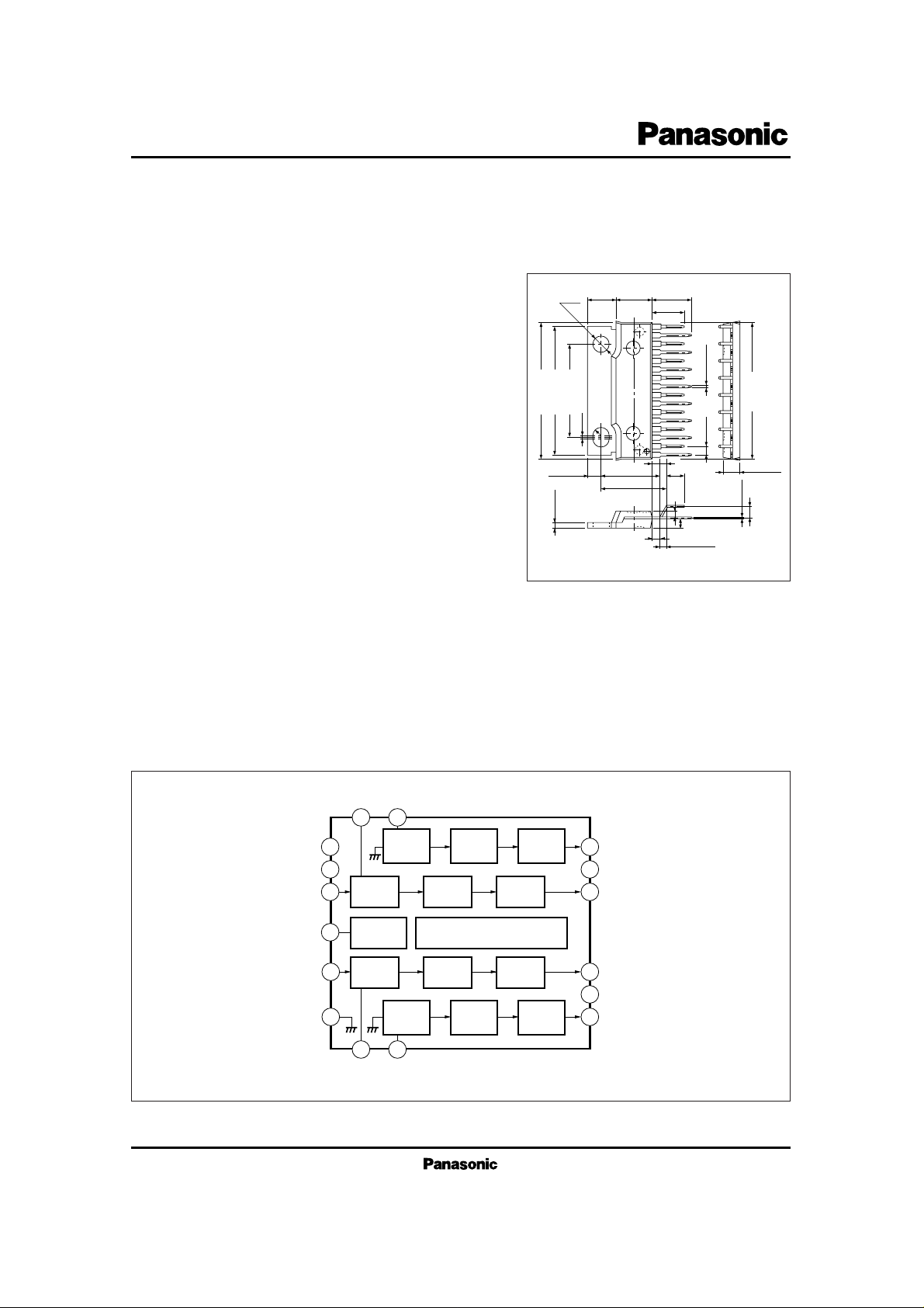
Unit : mm
6.33±0.5
29.6±0.3
5.9±0.25 7.7±0.3
7.8±0.5
1
16
29.96±0.3
0.6±0.21.778
ø 3.6
28.0±0.3
20.0±0.25
R1.8
0.6
1.2±0.1
3.5±0.3
2.66
2.8±0.3
12.5±0.3
(14.1)
(4.06)
2.54±0.8
(0.25)
1.45±0.25
1.8±0.25
(1.2)
1.45±0.25
Fin-attached 16-lead ZIP package (EZIP016-P-0660)
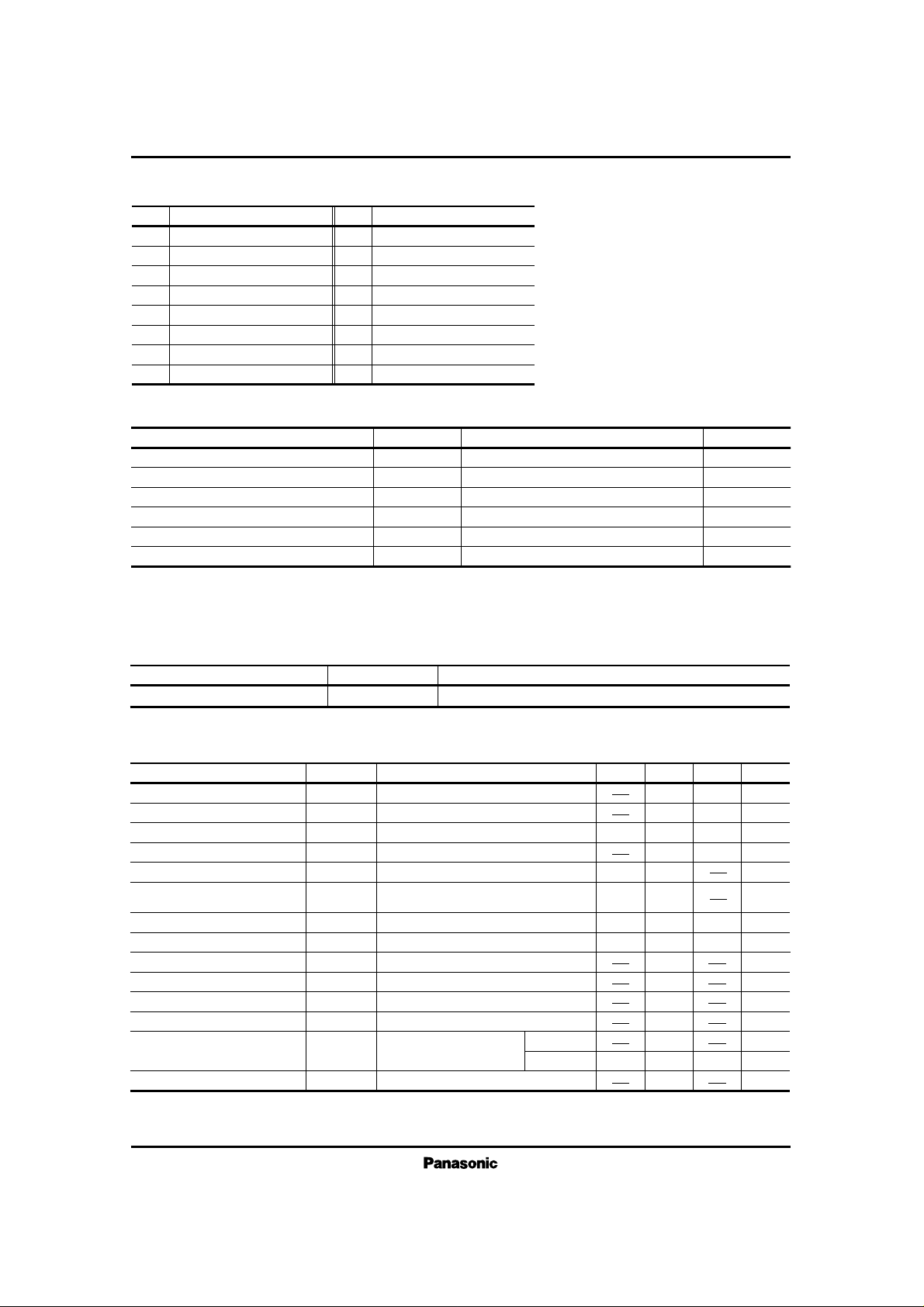
■ Block Diagram
1
13
6
5
12
10
11 9
14
15
16
4
3
2
87
V
CC
Ripple Filter
(Ch.1) IN
STAND-BY
(Ch.2) IN
GND
OUT (Ch.1) (+)
GND
OUT (Ch.1) (–)
OUT (Ch.2) (+)
OUT (Ch.2) (–)
GND
Input
Circuit
Driver
Circuit
Output
Circuit
Input
Circuit
Driver
Circuit
Output
Circuit
Input
Circuit
Driver
Circuit
Output
Circuit
Input
Circuit
Driver
Circuit
Output
Circuit
Stand-by
Circuit
Protection Circuit
NF
(Ch.2)NF(Ch.2)
NF (Ch.1) NF (Ch.1)
ICs for Audio Common Use
AN7171NK, AN7176K
Pin No.
Pin Name
1
2
3
4
5
6
7
8
V
CC
Output Ch.1 (+)
GND (Output Ch.1)
Output Ch.1 (–)
Stand-by
Input Ch.1
Negative Feedback Ch.1
Negative Feedback Ch.1
Pin No.
Pin Name
9
10
11
12
13
14
15
16
Negative Feedback Ch.2
GND (Input)
Negative Feedback Ch.2
Input Ch.2
Ripple Filter
Output Ch.2 (–)
GND (Output Ch.2)
Output Ch.2 (+)
■ Pin Descriptions
■ Absolute Maximum Ratings (Ta= 25˚C)
VCC
Note 1)
V
CC (surge)
Note 2)
I
CC
PD
Note 3)
T
opr
T
stg
Supply Voltage
Peak Supply Voltage
Supply Current
Power Dissipation
Operating Ambient Temperature
Storage Temperature
V
V
A
W
˚C
˚C
Parameter Symbol Rating Unit
24
50.0
6.0
37.5
Note 4)
– 30 ~ + 75
– 55 ~ + 150
Note 1) When no signals
Note 2) Time = 0.2s
Note 3) R
θj – c
= 2˚C/W
Note 4) Ta = 75˚C
■ Electrical Characteristics (V
CC
= 13.2V, RL= 4Ω, f = 1kHz, Ta = 25˚C)
Parameter Symbol Condition min. typ. max. Unit
Quiescent Current
Output Noise Voltage
Note)
Voltage Gain
Total Harmonic Distortion
Max. Output Power (4Ω)
mA
mVrms
dB
%
W
V
in
= 0mV
V
in
= 0mV, Rg= 10kΩ
V
in
= 5mV
V
in
= 5mV
THD= 10%
I
CQ
V
no
G
V
THD
P
O
Output Offset Voltage
Channel Balance
Total Harmonic Distortion
Total Harmonic Distortion
Frequency Characteristics
Frequency Characteristics
Crosstalk
Ripple Rejection Ratio
Note)
Vin= 5mV
V
in
= 5mV, 100Hz
V
in
= 5mV, 10kHz
V
in
= 5mV, –3dB down
V
in
= 5mV, –3dB down
RR
Rg= 0Ω
Rg= 0Ω, Vin= 0mV,
Ripple= 300mVrms, 120Hz
V
O (offset)
CB
THD
THD
f
CH
f
CL
I
STB
CT
Stand-by Pin ON
AN7171NK
AN7176K
V
in
= 5mV, Rg= 10kΩ
50.5
9.0
120
0.60
52.5
0.20
12.5
200
1.50
54.5
0.75
35 40
–200
–1
0
0
0.26
0.45
22
21
21
650
61
400
+ 200
+ 1
1000
dB
mV
dB
%
%
kHz
Hz
µA
µA
dB
Note) With 15Hz to 30kHz (12dB/OCT) filter
Stand-by Current
Parameter Symbol Range
■ Recommended Operating Range (Ta = 25˚C)
Operating Supply Voltage Range
V
CC
8.0V ~ 18.0V
 Loading...