

Panasonic AN7168 Datasheet

ICs for Audio Common Use
■ Overview
The AN7168 is an integrated circuit designed for low
distortion, low noise and low power dissipation audio set
of 5.8W (13.2V, 4Ω) output. Stereo operation is enabled
due to incorporating two amplifiers on one chip. 12-pin
SIL package enabled compact and high integrated set.
Thermal protection, short protection and excessive protection circuits are built in.
■ Features
•
Highly stable operation
•
Low distortion
•
Low quiescent current
•
Low noise
•
Low shock noise from power ON/OFF operation
•
Built-in muting circuit
•
Fewer external components
•
Incorporating protection circuits
AN7168
Dual 5.8W Audio Power Amplifier Circuit
29.96±0.3
29.6±0.3
12
1
Unit : mm
28.0±0.3
20.0±0.2
5.9±0.25 7.7±0.3 7.8±0.25
1.2±0.1
2.54
0.6±0.1
3.5±0.3
0.35
+ 0.1
– 0.05
ø 3.6
R1.8
0.6
12-Lead SIP Package with Fin (HSIP012-P-0000A)
■ Block Diagram
■ Pin Descriptions
Pin No.
Pin Name
1
2
3
4
5
6
NFB Ch.1
Input Ch.1
Ripple Filter
GND (Input)
Input Ch.2
NFB Ch.2
Pin No.
Pin Name
7
8
9
10
11
12
Output Ch.2
Bootstrap Ch.2
GND (Output)
V
CC
Bootstrap Ch.1
Output Ch.1
2
3
5
Input
Circuit
Input
Circuit
6 4 9 8
Driver
Circuit
Driver
Circuit
Over Voltage
Over Current
Over Temperature
Protection
GND (Output)GND (Input)
Output
Circuit
Output
Circuit
111
12
10
V
CC
7
AN7168
ICs for Audio Common Use
■ Absolute Maximum Ratings (Ta= 25˚C)
V
CC
I
CC
P
D
V
CC (surge)
T
opr
T
stg
Supply Voltage
Supply Current
Power Dissipation
Note 1)
Peak Supply Voltage
Note 2)
Operating Ambient Temperature
Storage Temperature
V
A
W
V
˚C
˚C
Parameter Symbol Rating Unit
24
4
41.7
50
– 30 ~ + 75
– 55 ~ + 150
Note 1) R
θ j – c
= 3˚C/W
Note 2) Voltage applied time = 0.2s
Vi= 0mV
P
O
= 0.5W
P
O
= 0.5W, f= 1kHz
P
O
= 0.5W, f= 100Hz
P
O
= 0.5W, f= 10kHz
THD = 10%
THD = 10%, R
L
= 2Ω
THD = 10%, R
L
= 8Ω
Rg= 10kΩ, 1000pF
f = 15Hz ~ 30kHz, 12dB/OCT
R
g
= 10kΩ, 1000pF, Without Filter
P
O
= 0.5W
P
O
= 0.5W
PO=
0.5W, Rg = 10kΩ, V
ripple
=
280mVrms
,
f
ripple
= 12Hz Sine wave
V
i
= 0mV
Parameter Symbol Condition min. typ. max. Unit
■ Electrical Characteristics (V
CC
= 13.2V, f = 1kHz, RL= 4Ω, Ta= 25˚C)
55
54
0.1
0.1
0.2
5.7
8.9
3.1
0.8
1.1
0
50
45
0
Quiescent Circuit Current
Voltage Gain
Total Harmonic Distortion
Maximum Output
Output Noise Voltage
Channel Balance
Channel Separation
Ripple Rejection Ratio
Offset Voltage
I
CQ
G
V
THD
P
O
V
no
CB
CS
RR
V
O (offset)
mA
dB
%
W
mV
dB
dB
dB
mV
30
52
5
40
35
100
56
0.5
1.5
1
200
50
40
30
20
10
0
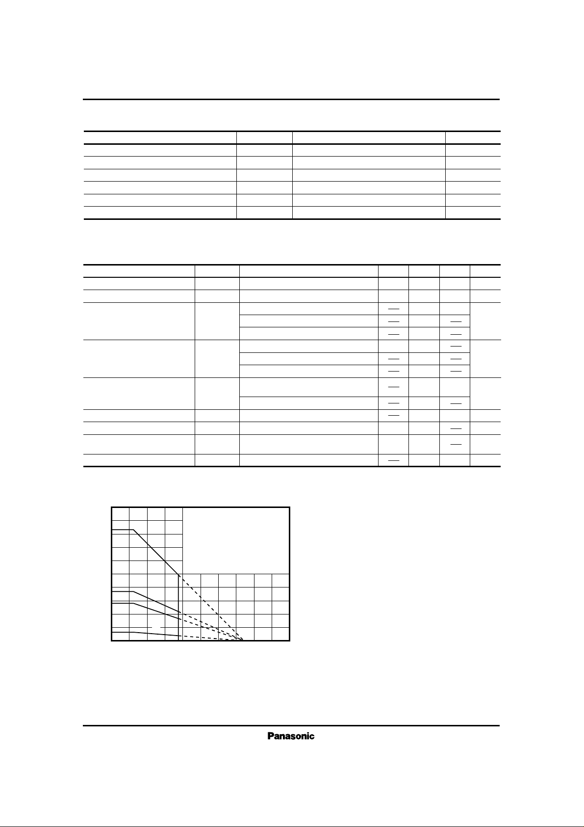
Ambient Temperature Ta (˚C)
Power Dissipation P
D
(W)
120
200
400
PD – Ta
80 160
(1)
(1) Tc= Ta (θ
j – c
= 3˚C/W)
(2) With a 100cm
2
× 3mm Al
heat sink (black color coated)
or a 200cm
2
× 2mm Al heat
sink (not lacquered)
(3) With a 100cm
2
× 2mm Al
heat sink (not lacquered)
(4) Without heat sink
(2)
(3)
(4)
 Loading...