Panasonic AN7158N Datasheet

ICs for Audio Common Use
■ Overview
The AN7158N is an integrated circuit designed for
power amplifier of 7.5W (16V, 4Ω) output with low noise
and low distortion, and it suits TV set with multi-sound.
Stereo operation is enabled due to incorporating two
amplifiers on one chip. 12-pin SIL package enabled compact and high-densely mounted set.
■ Features
•
Incorporating protection circuits (surge, thermal protec-
tion and etc.)
•
Automatic operating point stabilizer circuit
•
Low distortion, low 1/f noise
•
Low shock noise from power ON/OFF operation
•
Better channel separation
•
Fewer external components
AN7158N
Dual 7.5W Audio Power Amplifier Circuit
12
11
10
9
8
7
6
5
4
3
2
1
30.0±0.3
24.0±0.3
Unit : mm
1.26±0.25
1.8R
3.6±0.2
15.0±0.3 7.7±0.25 4.7±0.3
2.7±0.41.0±0.5
2.54
0.7±0.1
5.5±0.3
0.95±0.25
0.35±0.25
0.35
+ 0.1
– 0.05
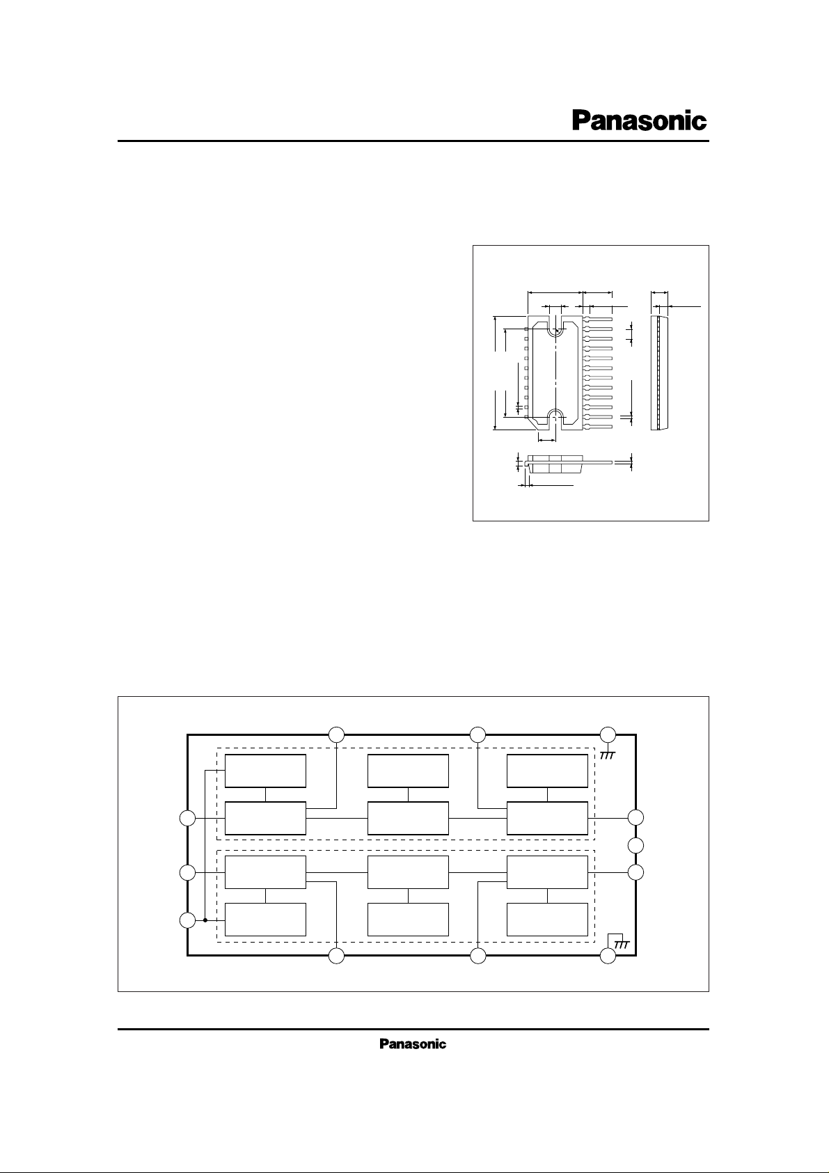
12-Lead SIP Package (HSIP012-P-0000B)
■ Block Diagram
9
4
12
5 6 3
11
1
2
8
V
CC
7 10
Ch.2 Bootstrap GND
Input Circuit Drive Output Circuit
Over Voltage
Protection
Temperature
Compensation
Shock Noise
Suppression
Input Circuit Drive
Over Voltage
Protection
Temperature
Compensation
Shock Noise
Suppression
Ch.1 Bootstrap
Ch.2
Input
Ch.1
Input
Ch.2
Output
Ch.1
Output
GND
Output Circuit

AN7158N
ICs for Audio Common Use
■ Absolute Maximum Ratings (Ta= 25˚C)
V
CC
V
CC
I
CC
P
D
T
opr
T
stg
Supply Voltage
Note 1)
Supply Voltage
Note 2)
Supply Current
Power Dissipation (Ta= 45˚C)
Operating Ambient Temperature
Storage Temperature
V
V
A
W
˚C
˚C
Parameter Symbol Rating Unit
24
20
4
30
– 30 ~ + 75
– 55 ~ + 150
Note 1) Without signal V
CC
= 24V (For non-stabilized supply)
Note 2) Operation VCC= 20V (For stabilized supply)
Quiescent Circuit Current
Voltage Gain
Output Power
Total Harmonic Distortion
Output Noise Voltage
Channel Balance
Separation
Ripple Rejection Ratio
I
CQ
G
V
P
O
THD
V
no
CB
Sep.
RR
Vi = 0mV
V
i
= 3mV
THD
= 10%
V
i
= 3mV
R
g
= 10kΩ
f
= 60Hz, Rg = 600Ω
40
52
4.8
45
70
54
5.5
0.15
1
0
50
40
120
56
1
3
1
mA
dB
W
%
mV
dB
dB
dB
Parameter Symbol Condition min. typ. max. Unit
• VCC=13.2V, RL= 4Ω, f =1kHz
Vi = 3mV
Quiescent Circuit Current
Voltage Gain
Total Harmonic Distortion
Output Noise Voltage
Crosstalk
I
CQ
G
V
THD
V
no
CT
V
i
= 0mV
V
i
= 4mV
THD
= 10%
R
L
= 4Ω, THD = 10%
V
i
= 4mV
R
g
= 10kΩ
V
i
= 4mV, Rg = 10kΩ
40
52
4
45
80
54
4.5
7.5
0.1
1
140
56
1
3
mA
dB
W
W
%
mV
dB
Parameter Symbol Condition min. typ. max. Unit
• V
CC
=16V, RL= 8Ω, f =1kHz
Output Power P
O
■ Electrical Characteristics (Ta = 25˚C)
40
36
32
28
24
20
16
12
8
4
0
Ambient Temperature Ta (˚C)
Power Dissipation P
D
(W)
140–20 40 80
(4)
20
(3)
(2)
(1)
180160120100600
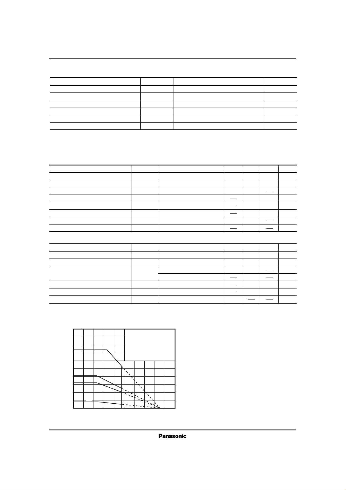
PD – Ta
(1) Tc = Ta
(2) With a 100cm
2
× 3mm
Al heat sink (black)
or a 200cm
2
× 2mm
Al heat sink
(3) With a 100cm
2
× 2mm
Al heat sink
(4) Without heat sink
 Loading...