

Panasonic AN7148 Datasheet
ICs for Audio Common Use
■ Overview
The AN7148 is an integrated circuit designed for power
amplifier of 2.1W (9V, 4Ω) output. Stereo operation is
enabled due to incorporating two amplifiers on one chip.
It is most suitably used for battery operated set such as
radio cassette recorder because quiescent circuit current
is small comparing to current power amplifier. Low distortion and low noise are realized and external components
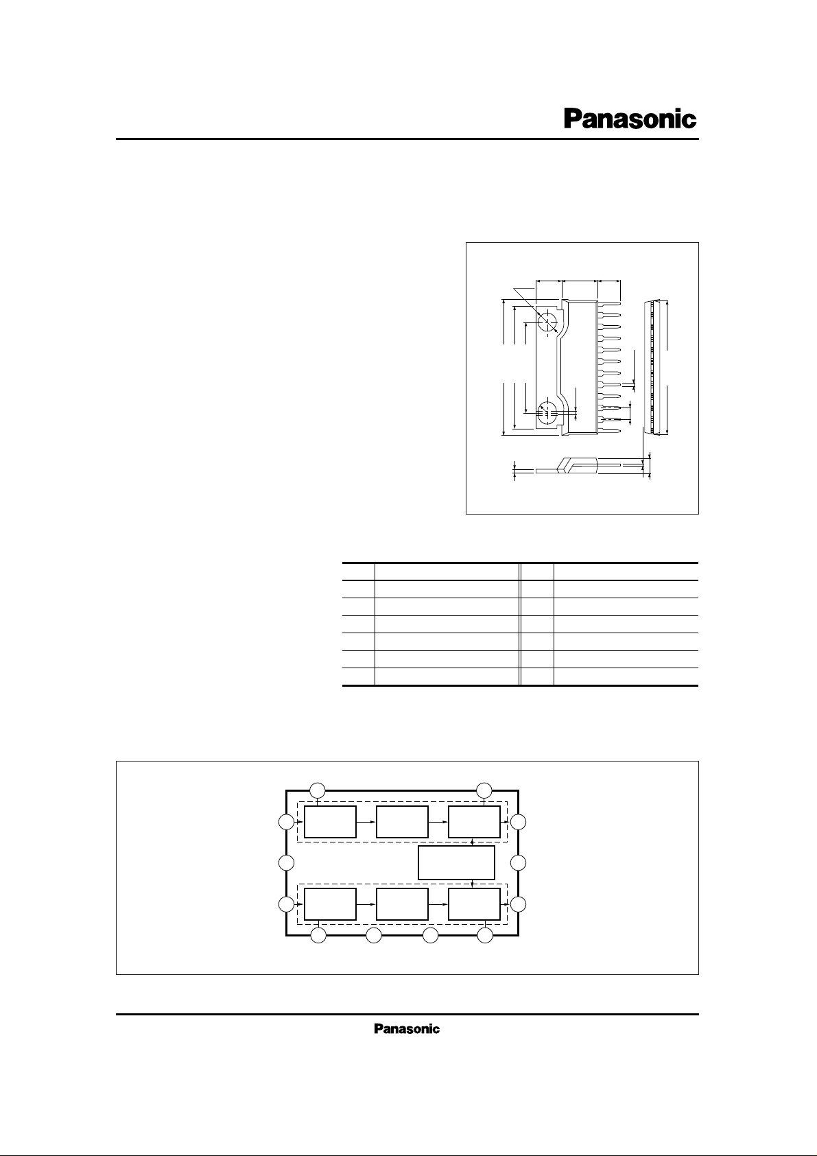
are very few. 12-pin SIL package has realized compact
and high density mounting of a set.
■ Features
•
Low quiescent current
•
High operation stability
•
Low radiation
•
Low distortion
•
Low noise
•
Low shock noise from power ON/OFF operation
•
Fewer external components
AN7148
Dual 2.1W Audio Power Amplifier Circuit
29.96±0.3
29.6±0.3
12
1
Unit : mm
28.0±0.3
20.0±0.2
5.9±0.25 7.7±0.3 7.8±0.25
1.2±0.1
2.54
0.6±0.1
3.5±0.3
0.35
+ 0.1
– 0.05
ø 3.6
R1.8
0.6
12-Lead SIP Package with Fin (HSIP012-P-0000A)
■ Block Diagram
Input
Circuit
Driver
Circuit
Output
Circuit
V
CC
1 11
2
3
6 4 9 8
12
10
GND (Output)GND (Input)
5 7
Input
Circuit
Driver
Circuit
Output
Circuit
Over Temperature
Protection
Ch.1
Ch.2
■ Pin Descriptions
Pin No.
1
N.F.B Ch.1
2
Input Ch.1
3
Ripple Filter
4
GND (Input)
5
Input Ch.2
6
N.F.B Ch.2
Pin Name
Pin No.
7
8
9
10
11
12
Pin Name
Output Ch.2
Bootstrap Ch.2
GND (Output)
V
CC
Bootstrap Ch.1
Output Ch.1
ICs for Audio Common Use
AN7148
V
CC
I
CC
PD
*
T
opr
T
stg
Supply Voltage
Supply Current
Power Dissipation
Operating Ambient Temperature
Storage Temperature
V
A
W
˚C
˚C
Parameter Symbol Rating Unit
24
3.5
41.7
– 30 ~ + 75
– 55 ~ + 150
■ Absolute Maximum Ratings (Ta= 25˚C)
*
R
θ j – c
= 3˚C/W
Output Noise Voltage
Voltage Gain (Gain)
Total Harmonic Distortion
Maximum Output Power (4Ω)
Channel Balance
Maximum Output Power (8Ω)
Maximum Output Power (3Ω)
V
no
*
G
V
THD
P
O (max.)
CB
P
O (max.) 8
P
O (max.) 3
V
CC
= 9V, RL = 4Ω, V
in
= 0mV,
Rg = 10kΩ
42.5
1.75
0.25
44.5
0.20
2.10
0
1.25
2.6
0.50
46.5
0.75
1
mV
dB
%
W
dB
W
W
Parameter Symbol Condition min. typ. max. Unit
Note) Operating Supply Voltage Range : V
CC (opr.)
= 6 ~ 18V
*
Filter with band width of 15Hz ~ 30kHz (12dB/oct) should be used for Vno measurement.
Quiescent Circuit Current I
CQ
V
CC
= 9V, RL = 4Ω, V
in
= 0mV 13 19 mA
V
CC
= 9V, RL = 4Ω, V
in
= 3mV,
f = 1kHz
V
CC
= 9V, RL = 4Ω, V
in
= 3mV,
f = 1kHz
V
CC
= 9V, RL = 4Ω,
THD = 10%, f = 1kHz
V
CC
= 9V, RL = 4Ω, V
in
= 3mV,
f = 1kHz
V
CC
= 9V, RL = 8Ω,
THD = 10%, f = 1kHz
V
CC
= 9V, RL = 3Ω,
THD = 10%, f = 1kHz
■ Electrical Characteristics (Ta = 25˚C)
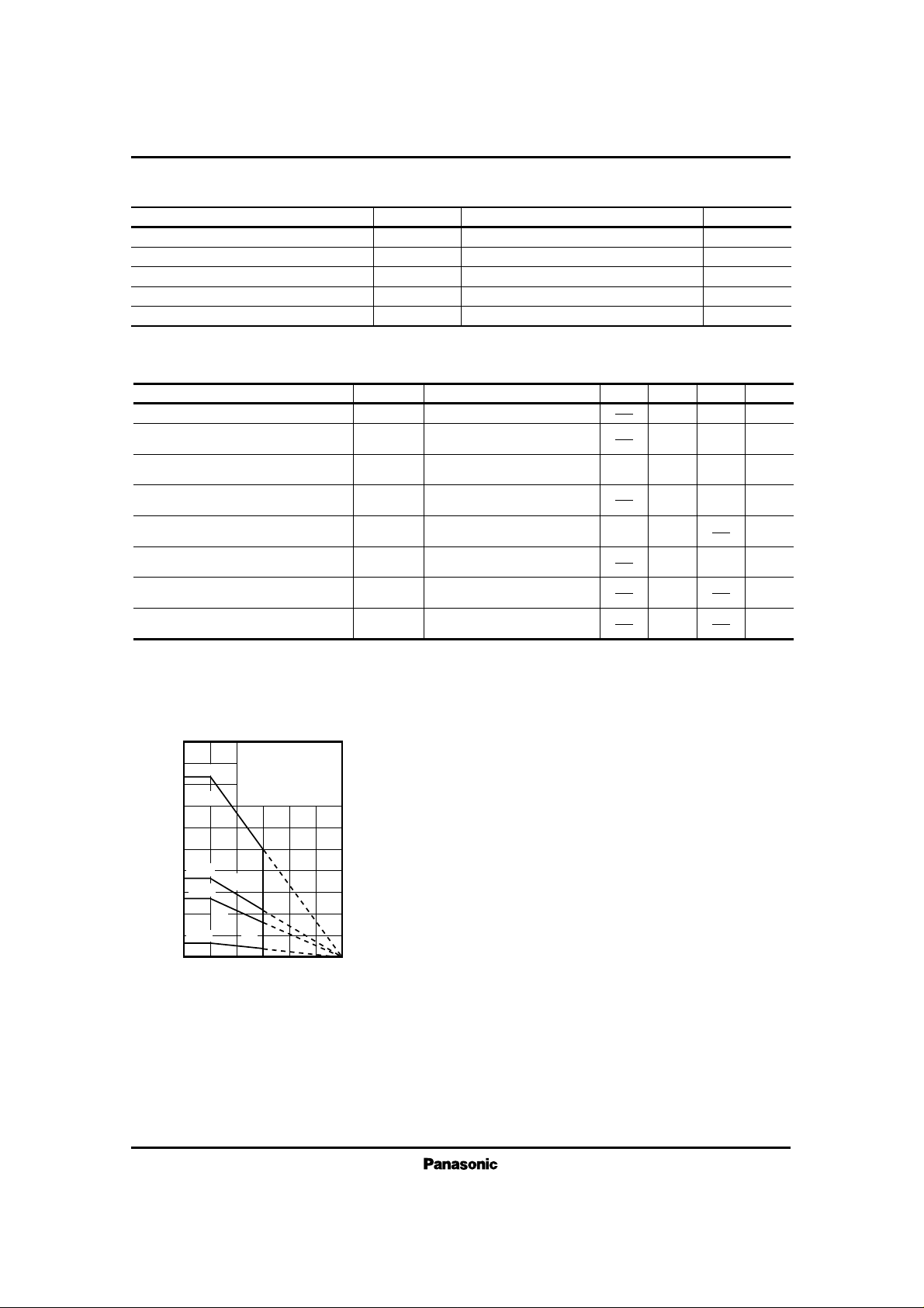
PD – Ta
50
45
40
35
30
25
20
15
10
5
0
Ambient Temperature Ta (˚C)
Power Dissipation P
D
(W)
750 25 50 100 125
150
(1)
(3)
(4)
41.7W
17.9W
13.9W
3.0W
(2)
(1) Tc = Ta (θ
j– c
= 3˚C/W)
(2) With a 100cm
2
× 3mm Al
heat sink (black color coated)
or a 200cm
2
× 2mm Al heat
sink (not lacquered)
(3) With a 100cm
2
× 2mm Al
heat sink (not lacquered)
(4) Without heat sink
 Loading...