Panasonic AN7135 Datasheet

ICs for Audio Common Use
■ Overview
The AN7135 is a power amplifier circuit of 7.5W (15.0V,
3Ω) output. It can provide stereo operation since two
amplifiers are incorporated in a chip. Static circuit current
is very smaller than conventional IC for power amplifier,
and various protective circuits are incorporated, thus providing high reliability. For its feature of very small static
circuit current, it is best suitable for dry cell operating sets
(e.g. radio cassette recorder). It requires smaller number
of external components because it has little distortion and
low noise and can support the stand-by condition.
■ Features
•
Small static circuit current
•
Stand-by condition supported
•
Good oscillation stability
•
Little unwanted radiation to RF portion of AM/FM
•
Little distortion
•
Low noise
•
Small shock noise at power ON/OFF, stand-by ON/OFF
•
Fewer external components
AN7135
Dual 7.5W Low Frequency Power Amplifier Circuit
29.96±0.3
29.6±0.3
12
1
Unit : mm
28.0±0.3
20.0±0.2
5.9±0.25 7.7±0.3 7.8±0.25
1.2±0.1
2.54
0.6±0.1
3.5±0.3
0.35
+ 0.1
– 0.05
ø 3.6
R1.8
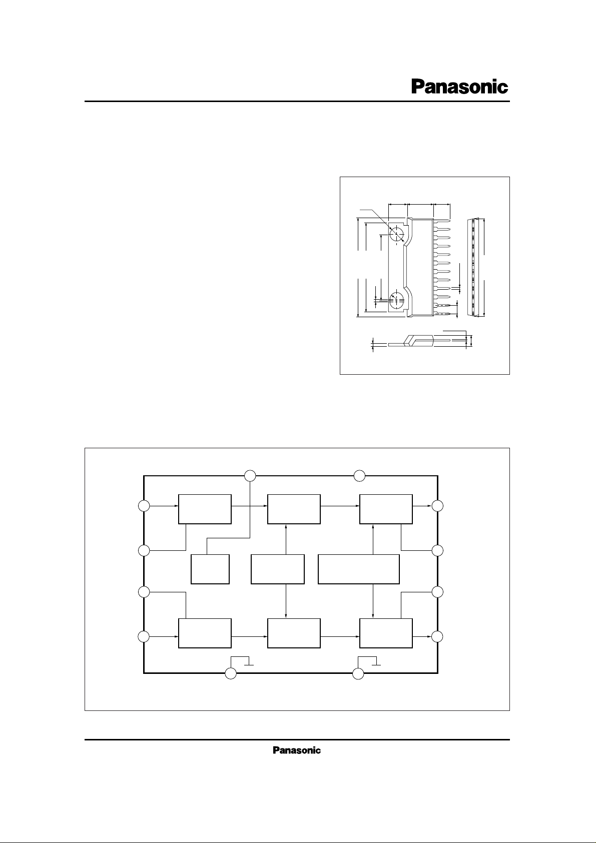
Fin-attached 12-lead SIP package (HSIP012-P-0000A)
0.6
■ Block Diagram
2
1
6
5
3
Input Circuit
Bias Circuit
Input Circuit Drive Circuit
4
GND
(Input)
Drive Circuit
Over Temperature
Protection
V
CC
10
Crossover
Distortion
9
GND
(Output)
SEPP
Output Circuit
SEPP
Output Circuit
12
11
8
7

ICs for Audio Common Use
AN7135
Pin No.
Pin Name
1
2
3
4
5
6
Negative Feedback Ch.1
Input Ch.1
Ripple filter/Stand-by Controller
GND (Input)
Input Ch.2
Negative Feedback Ch.2
■ Pin Name
Pin No.
Pin Name
7
8
9
10
11
12
Output Ch.2
Boot-strap Ch.2
GND (Output)
V
CC
Boot-strap Ch.1
Output Ch.1
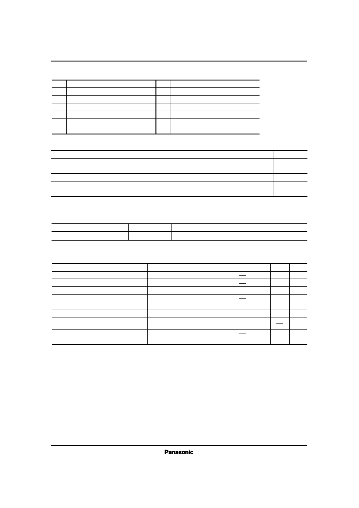
■ Absolute Maximum Ratings (Ta= 25˚C)
V
CC
I
CC
P
D
T
opr
T
stg
Supply Voltage
Supply Current
Power Dissipation
Note 1)
Operating Ambient Temperature
Storage Temperature
V
A
W
˚C
˚C
Parameter Symbol Rating Unit
24
4
62.5
– 30 ~ + 75
– 55 ~ + 150
Note) θ
j–c
= 2˚C/W
Parameter Symbol Range
■ Recommended Operating Range (Ta= 25˚C)
Operating Supply Voltage Range
V
CC
5.5V ~ 18.0V
Note) 24V at no signals
Parameter Symbol Condition min. typ. max. Unit
■ Electrical Characteristics (V
CC
= 15V, f
IN
= 1kHz, RL = 3Ω, Both channel drive, Ta= 25˚C ± 2˚C)
Quiescent Current
Output End Noise Voltage
Note 1)
Voltage Gain
Total Harmonics Distortion
Max. Output Power
Channel Balance
mA
mV
dB
%
W
dB
V
IN
= 0mV
V
IN
= 0mV, Rg= 10kΩ
V
IN
= 3mV
V
IN
= 3mV
THD= 10%
V
IN
= 3mV
I
CQ
V
NO
G
V
THD
P
O
CB
Input Offset Voltage
Stand-by Current
Ripple Rejection Ratio
Note 1)
RR
Input pin open
Pin3 open
V
CC (ripple)
= 280mV, f
(ripple)
= 120Hz
R
g
= 0Ω Sine wave
V
IN (O.S)
I
STB
42.5
7.0
–1
14
0.25
44.5
0.40
7.5
0
20
0.50
46.5
0.75
45 50
+ 1
10
30
30
dB
mV
µA
Note 1) Measured through 15Hz to 30kHz (12dB/OCT) filter
 Loading...