Panasonic AN7118S Datasheet

ICs for Audio Common Use
■ Overview
The AN7118S is the ICs designed for power amplifier of
low voltage operated compact radio and stereo tape
recorder. Stereo operation is enabled due to incorporating two amplifiers on one chip. Miniaturization of cassette
and high integration is realized due to SOP package.
■ Features
•
Low voltage operation : V
CC
= 1.8V to 4.5V
•
Reduced voltage operation is available.
•
Low pop noise when supply voltage is switched ON
and OFF
•
Stereo drive of 4Ω (speaker) to 32Ω (headphone) load
is possible.
AN7118S
Low Voltage Dual 35mW Audio Power Amplifier Circuits (BTL 300mW)
1.3
0.4±0.25
1.27
0.1±0.1
0.3
1.5±0.2
0.65
0.15
1
2
3
4
5
6
7
8
9
18
17
16
15
14
13
12
11
10
18-Lead SOP Package (SOP018-P-0300)
12.6±0.3
7.7±0.3
5.4±0.3
Unit : mm
■ Block Diagram
V
CC
18 7 6 5 4 9
3
N.C
Input
Amp.
8
Input (1)
Input (2)
11
16N.C
Input
Amp.
10 12 13 14 15 1
GND (Input) GND (Output)
Driver
Driver
SEPP
Output Amp.
Output (1)
Output (2)
SEPP
Output Amp.
2
17

ICs for Audio Common Use
AN7118S
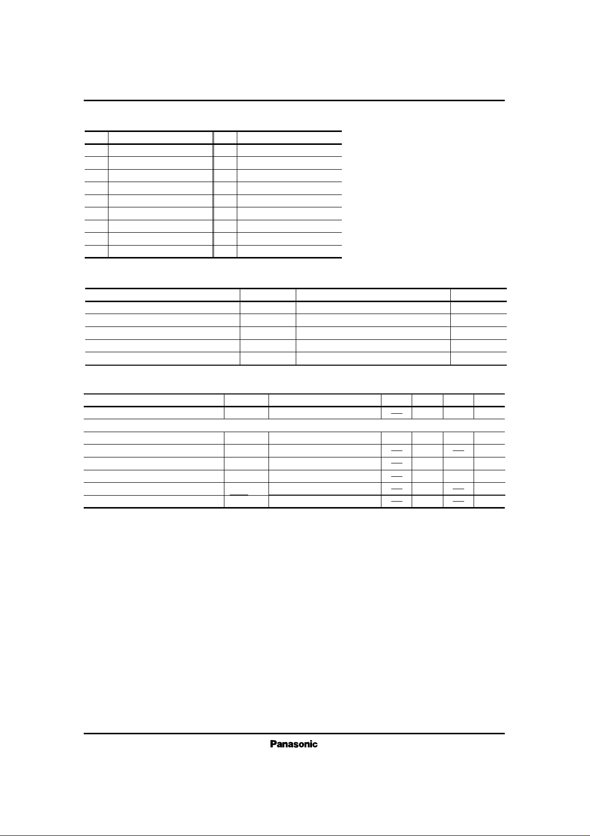
■ Absolute Maximum Ratings (Ta= 25˚C)
V
CC
I
CC
P
D
T
opr
T
stg
Supply Voltage
Supply Current
Power Dissipation
Operating Ambient Temperature
Storage Temperature
V
A
mW
˚C
˚C
Parameter Symbol Rating Unit
4.5
1
400
– 20 ~ + 75
– 50 ~ + 125
■ Pin Descriptions
Pin No.
Pin Name
1
2
3
4
5
6
7
8
9
GND (Output)
Output Ch.1
NC
Bootstrap
Phase Compensation
Phase Compensation
N.F.B
Input Ch.1
V
CC
Pin No.
Pin Name
10
11
12
13
14
15
16
17
18
GND (Input)
Input Ch.2
N.F.B
Phase Compensation
Phase Compensation
Bootstrap
NC
Output Ch.2
Ripple Filter
■ Electrical Characteristics (V
CC
= 3V, Ta = 25˚C)
Vi= 0mV
V
i
= 1.5mV, RL= 32Ω
THD = 10%, R
L
= 32Ω × 2ch.
V
i
= 1.5mV, RL= 32Ω × 2ch.
R
g
= 10kΩ, DIN Audio Filter
V
CC
= 3V± 200mV, f= 100Hz
Parameter Symbol Condition min. typ. max. Unit
13
47
33
0.3
0.5
20
35
Quiescent Circuit Current
<DUAL (f=1kHz)>
Voltage Gain
Maximum Output
Total Harmonic Distortion
Output Noise Voltage
Input Resistance
Ripple Rejection Ratio
I
CQ
G
V
P
O
THD
V
no
Ri
RR
mA
dB
mW
%
mW
kΩ
dB
45
18
49
1
1
 Loading...