

Panasonic AN7090FHQ Datasheet
ICs for Information Equipment
AN7090FHQ
Peripheral analog IC for audio signal processing
■ Overview
The AN7090FHQ is a one chip IC of audio signal
processing analog circuit for use in various information
systems including microcomputer.
Small-sizing of system and low power dissipation are
possible.
■ Features
• Built-in head phone amplifier
• Built-in external/internal microphone switching circuit
• Enables power save mode
■ Applications
• Note-type personal computer, desk-top personal com-
puter, portable information terminal and others
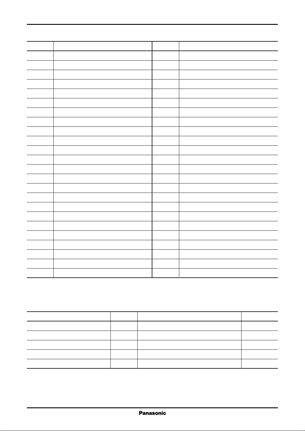
■ Block Diagram
COGN
GND
CDR1
CDR2
CIGN
CDL1
CDL2
PV
DD
NV
DD
GND
HPOL
PGND
SPOL
37
38
39
40
41
42
43
44
45
46
47
48
CDOR
36
POW
0 dB
1
PON
CDOL
35
34
0 dB
0 dB
0 dB 0 dB
2
3
LOIL
OUTL
33
4
VINL
MDET
32
Mute
5
MOUT
MICO
31
6
DD
NV
MGAI
30
7
DD
PV
MSEL
29
47 dB
8
SENB
36 25
37
1
(0.75)
IMIC
28
43 dB
27 dB
9
VINR
9.00±0.40
7.00±0.20
MGND
27
10
LOIR
0.50
Seating plane
EMIC
26
23 dB
POW
0 dB
11
OUTR
24
(0.75)
7.00±0.20
1348
12
+0.10
0.20
–0.05
1.40±0.10
(0.625)(0.625)
0.10±0.10
LQFP048- P-0707
RE
MV
25
24
MV
23
LINL
22
LINR
21
20
19
18
17
16
15
14
13
GND
LIJR
LIJL
NV
GND
PV
HPOR
GND
SPOR
0 dB0 dB
12
PGND
Unit : mm
9.00±0.40
5
0
.0
.1
0
0
–
+
1.70 max.
0.15
DD
DD
DD
(1.00)
0° to 10°
0.50±0.20
1
AN7090FHQ ICs for Information Equipment
■ Pin Descriptions
Pin No. Description
1 Power on control
2 Line-out jack L-channel
3 Line-out input L-channel
4 VR-input L-channel
5 Mono out
6 −5VDD (power)
7 +5VDD (power)
8 Speaker enable
9 VR-input R-channel
10 Line-out input R-channel
11 Line-out jack R-channel
12 Power GND
13 Speaker-out R-channel
14 GND (power)
15 Headphone-out R-channel
16 +5V
DD
17 GND
18 −5V
DD
19 Line-in jack L-channel
20 Line-in jack R-channel
21 GND
22 Line-in output R-channel
23 Line-in output L-channel
24 Mic. amp. V
DD
Pin No. Description
25 Mic. V
REF
26 External mic. input
27 Mic. GND
28 Internal mic. input
29 Mic. select (int./ext.)
30 Mic. gain
31 Mic. output
32 Mic. mute
33 Mic. NF
34 CD-out L-channel
35 CD-out GND
36 CD-out R-channel
37 GND
38 CD-in R-channel 1
39 CD-in R-channel 2
40 CD-in GND
41 CD-in L-channel 1
42 CD-in L-channel 2
43 +5V
44 −5V
DD
DD
45 GND
46 Headphone-out L-channel
47 Power GND
48 Speaker-out L-channel
■ Absolute Maximum Ratings
Parameter Symbol Rating Unit
Supply voltage V
Supply current I
2
Power dissipation
Operating ambient temperature
Storage temperature
Note)*1: Ta = 25°C except operating ambient temperature and storage temperature.
2: Ta = 75°C
*
*
1
*
1
*
CC
CC
P
D
T
opr
T
stg
2
±6V
15 mA
180 mW
−20 to +70 °C
−55 to +125 °C

ICs for Information Equipment AN7090FHQ
■ Recommended Operating Range
Parameter Symbol Range Unit
Supply voltage V
CC
■ Electrical Characteristics at VCC = ±5 V, f = 1 kHz, Ta = 25°C
Parameter Symbol Conditions Min Typ Max Unit
Line-out jack block
1
Line-out gain
*
Line-out total harmonic distortion
Line-out output residual noise
1
Cross talk 1
*
*
Speaker-out block
1
Sp-out gain
*
Sp-out total harmonic distortion 2
2
Sp-out residual noise
Sp-out mute attenuation 1
Cross talk 2
*
*
1
*
1
Headphone amplifier block
1
Rated output
*
HP-out total harmonic distortion 3
2
HP-out residual noise
HP-out mute attenuation 2
1
Cross talk 3
*
*
1
*
Line-in jack block
1
L-jack gain
*
L-jack total harmonic distortion 4
2
L-jack output residual noise
1
Cross talk 4
*
*
CD-ROM block
1
CD in gain
*
CD in total harmonic distortion 5
2
CD in output residual noise
1
Cross talk 5
Note)*1 : Using the DIN audio filter.
*
2 : Using the A curve filter.
*
*
VLOLRVIN = 1 V[rms], f = 1 kHz −10 1
1
*
VLOTH VIN = 1 V[rms], f = 1 kHz 0.01 0.02
2
VLOSN VIN = 0 V[rms], Rg = 4.7 kΩ−90 −80
CT1 VIN = 1 V[rms], f = 1 kHz −70 −60
VSPLRVIN = 1 V[rms], f = 1 kHz −10 1
1
*
VSPTH VIN = 1 V[rms], f = 1 kHz 0.01 0.02
VSPSN VIN = 0 V[rms], Rg = 4.7 kΩ−85 −80
VMU1 VIN = 1 V[rms], f = 1 kHz −85 −80
CT2 VIN = 1 V[rms], f = 1 kHz −70 −60
HP
f = 1 kHz, distortion : 1%,
THD4
load : 32 Ω
1
*
THD3 VIN = 1 V[rms], f = 1 kHz,
load : 32 Ω
= 0 V[rms], f = 1 kHz, −85 −80
V
HS/N
IN
Rg = 4.7 kΩ, load : 32 Ω
V
= 1 V[rms], f = 1 kHz, −85 −80
VMU2
IN
load : 32 Ω
V
= 1 V[rms], f = 1 kHz, −70 −60
CT3
IN
load : 32 Ω
VLJ VIN = 1 V[rms], f = 1 kHz −10 1
1
*
THDJ VIN = 1 V[rms], f = 1 kHz 0.01 0.02
LJSN VIN = 0 V[rms], Rg = 4.7 kΩ−90 −80
CT4 VIN = 1 V[rms], f = 1 kHz −70 −60
VCDIN VIN = 1 V[rms], f = 1 kHz −10 1
1
*
CDTHD5
VIN = 1 V[rms], f = 1 kHz 0.01 0.02
CDSN VIN = 0 V[rms], Rg = 4.7 kΩ−85 −80
CT5IN VIN = 1 V[rms], f = 1 kHz −70 −60
±4.5 to ±5.0 typ. to ±5.5 V
dB
%
dB
dB
dB
%
dB
dB
dB
80 100 120 mW
0.01 0.02 %
dB
dB
dB
dB
%
dB
dB
dB
%
dB
dB
3

AN7090FHQ ICs for Information Equipment
■ Electrical Characteristics at VCC = ±5 V, f = 1 kHz, Ta = 25°C (continued)
Parameter Symbol Conditions Min Typ Max Unit
Internal-mic. block
1
Mic.-out voltage 1
Mic.-out voltage 2
Mic.-out output residual noise
*
1
*
2
*
Mic.-out total harmonic distortion 6
1
Mic.-out mute attenuation 3
*
External-mic. block
1
Mic.-out voltage 1
Mic.-out voltage 2
Mic.-out output residual noise
*
1
*
2
*
Mic.-out total harmonic distortion 7
1
Mic.-out mute attenuation 4
Mic. use V
Mic. use V
Mic. use V
voltage
REF
DC voltage
REF
voltage ripple noise
REF
*
1
*
Circuit current
Circuit current at no load 1 I
Circuit current at no load 2 I
Circuit current at power save 1 I
Circuit current at power save 2 I
Low-level mic. balance MICBL V
High-level mic. balance MICBH V
Note)*1 : Using the DIN audio filter.
2 : Using the A curve filter.
*
1
*
VMIMU1
1
*
VMIMU2
MICV
1
*
V
INT0VIN
V
INT1VIN
MICSN1
THDM6
V
EXT0VIN
V
EXT1VIN
MICSN2
THDM7
REFDC
MICV
REFRI
TOTA1
TOTA2
PWON1
PWON2
= 3 mV[rms], f = 1 kHz 0.3 0.7 1 V[rms]
= 3 mV[rms], f = 1 kHz 0.03 0.07 0.1 V[rms]
VIN = 0 V[rms], Rg = 2.2 kΩ−80 −75
dB
VIN = 25 mV[rms], f = 1 kHz 0.02 0.1 %
VIN = 3 mV[rms], f = 1 kHz −75 −70
dB
= 5 mV[rms], f = 1 kHz 0.3 0.7 1 V[rms]
= 5 mV[rms], f = 1 kHz 0.03 0.07 0.1 V[rms]
VIN = 0 V[rms], Rg = 2.2 kΩ−80 −75
dB
VIN = 25 mV[rms], f = 1 kHz 0.02 0.1 %
VIN = 5 mV[rms], f = 1 kHz −75 −70
dB
Flow out current at pin 25 : 2.3 2.5 2.7 V
3.3 mA
Flow out current at pin 25 : 0.01 V[p-p]
3.3 mA
No input signal (+VCC side) 5 7 10 mA
No input signal (−VCC side) 5 7 10 mA
No input signal (+VCC side) 0.3 1 5 mA
No input signal (−VCC side) 0.3 1 5 mA
EXT1
EXT0
− V
− V
INT1
INT0
030
0 200
mV[rms]
mV[rms]
4

ICs for Information Equipment AN7090FHQ
■ Terminal Equivalent Circuits
Pin No. Equivalent circuit Description
1 PON :
Switching control pin of power
save mode
1
1.3 V 1.6 V
−V
CC
−V
CC
−V
CC
0.8 V
−V
CC
2 OUTL : 0
V
CC
Output pin of L-channel lineout jack
500 Ω
2
Pin voltage
(V)
100 kΩ
−V
CC
3 LOIL : 0
V
CC
47
Input pin of L-channel line-out
jack
3
20 kΩ
−V
CC
47
5
 Loading...