

Panasonic AN7017SB Datasheet
ICs for FM/AM Tuner
■ Overview
The AN7017S and the AN7017SB are the ICs incorporating FM/TV front-end most suitable for headphone
stereo.
Sealed in a 16-pin flat package, the chip operates stably at TV band (170MHz ~ 222MHz) FM band (76MHz ~
108MHz).
RF amplifiers and oscillations are provided in FM/TV
band individually, and are designed most suitably. So
both characteristics of FM/TV band are satisfied.
■ Features
•
Low current consumption
•
Band switching circuit built-in
•
A single chip integrating FM/TV band
•
IF amp. built-in
AN7017S, AN7017SB
FM/TV Front-end ICs for 1.5V Headphone Stereo, Radio Cassette Recorder
■ Block Diagram
0.1±0.1
1.5±0.2
0.3
0.65
0.15
0.4
1
2
3
4
5
6
7
8
16
15
14
13
12
11
10
9
0.4±0.25
1.27
Unit : mm
6.5
±0.3
4.2±0.3
10.1±0.3
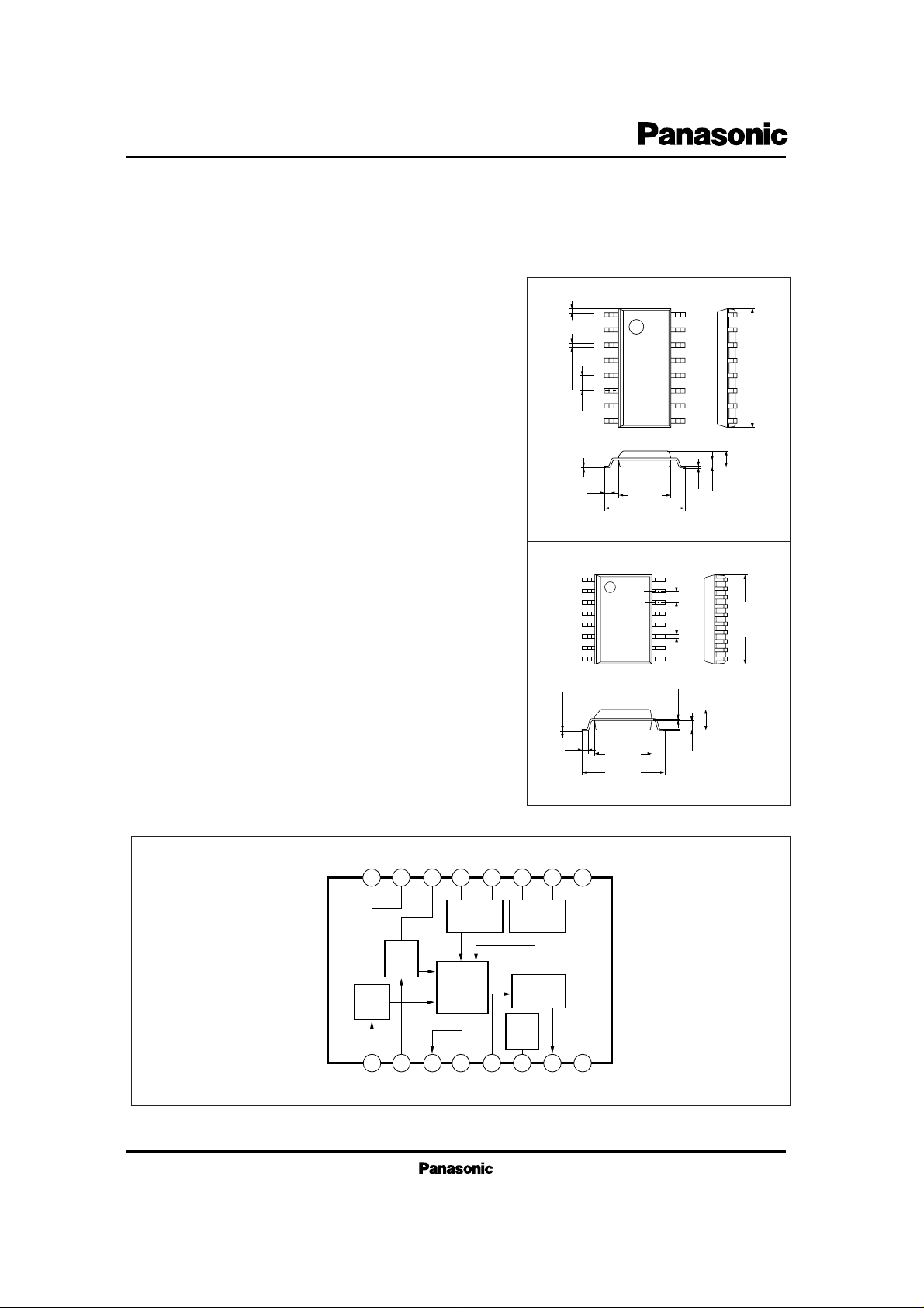
AN7017S
16-Lead SOP Package (SOP016-P-0225)
0.8
0.1±0.1
1.5±0.2
0.35±0.1
0.5
0.65
0.15
1
8
16
9
Unit : mm
6.5±0.3
6.3±0.3
4.3±0.3
AN7017SB
16-Lead SOP Package (SSOP016-P-0225a)
V
CC1
16 15 14 13 12 11 10 9
FM
L – OSCTVL – OSC
TV
RF
Amp.
FM
RF
Amp.
1 2 3 4 5 6 7 8
Mix.
GND
IF Amp.
TV/
FM
SW
V
CC2
GND

ICs for FM/AM Tuner
AN7017S, AN7017SB
■ Characteristics Curve
V
CC
I
CC
P
D
T
opr
T
stg
Supply Voltage
Supply Current
Power Dissipation
Operating Ambient Temperature
Storage Temperature
V
mA
mW
˚C
˚C
Parameter Symbol Rating Unit
■ Absolute Maximum Ratings (Ta=25˚C)
2.5
10
30
–22 ~ + 75
–55 ~ + 125
Parameter Symbol Range
■ Recommended Operating Range (Ta=25˚C)
Operating Supply Voltage Range
V
CC
1V ~ 2V
Parameter Symbol Condition min. typ. max. Unit
■ Electrical Characteristics (V
CC
=1.2V, Ta = 25˚C)
No Signal Current
Conversion Gain
Oscillation Voltage
S/N
No Signal Current
Conversion Gain
Oscillation Voltage
S/N
FM
TV
I
tot
(FM)
G
conv
(FM)
V
OSC
(FM)
S/N (FM)
I
tot
(TV)
G
conv
(TV)
V
OSC
(TV)
S/N (TV)
Note)
V
CC
=1V
V
in
= 60dBµ
2.5
31
73
55
3.2
27
57
53
mA
dB
mV
dB
mA
dB
mV
dB
Note)
V
CC
=1V
V
in
=60dBµ
Note) Conversion Gain= 20log (∆V
(µV)
÷100)
∆V is output difference at 40dBµ and 46dBµ.
Supply Voltage Characteristics (FM)–
Oscillation Frequency Deviation
S/N, S/N Sensitivity, Limiter Sensitivity, I
tot
0
0
50
60
70
80
90
100
1.0
VCC (V)
Limit Sens (dBµ), S/N Sens (dBµ), S/N (dB)
40
30
20
10
1.2 1.4 1.6 1.8 2.0 2.22.4 2.6 2.8 3.0
2
1
0
–1
–2
–3
4
3
2
I
tot
(mA)
f
sift
× 10
2
(kHz)
S/N
f
sift
Input/Output Characteristics –
S/N, V
out
0
–50
–40
–30
–20
–10
0
20
V
in
(dBµ)
V
out
(dB)
–60
40 60 80 100
60
50
40
30
20
10
0
S/N (dB)
V
out
120
0
0
20
30
40
50
60
70
78
Frequency f
in
(MHz)
S/N Sens (dBµ), Limit Sens (dBµ)
10
82 86 90
100
50
0
V
OSC
(mV)
98
Frequency Characteristics
(FM) –V
OSC
, S/N Sensitivity,
Limiter Sensitivity
102 10694
80
VCC = 1.2V
Ta = 25˚C
V
OSC
VCC = 1.5V
f
in
= 78MHz
30% Mod.
Ta = 25˚C
Ta =25˚C
S/N Sens
S/N Sens
Limit Sens
S/N
I
tot
Limiter Sens
 Loading...