ICs for Timer
AN6783S
IC for long interval timer
■ Overview
The AN6783S is an IC designed for a long interval
timer. It is oscillated by using the external resistor and
capacitor, and the oscillation frequency divided by a 15stage F.F. is provided as the output.
It is frequency divider type, so that a long interval
timer can be constructed by using a capacitor with small
capacitance.
■ Features
• Oscillation frequency dispersion of IC itself is small (±5
%)
• Oscillation frequency can be checked by 1/2 f
OSC
moni-
tor terminal
• Wide operating supply voltage range (3.2 V to 18 V)
• Small consumption current (3 mA typ.)
■ Applications
• Timer
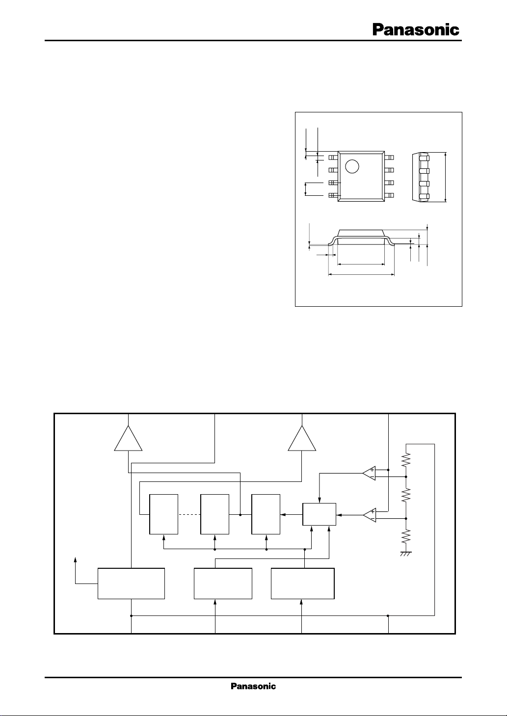
■ Block Diagram
CC
Mon.
8
V
7
6
0.6±0.3
1.27
0.1±0.1
Out
0.4±0.25
1
2
3
4
0.3
8
7
6
5
4.2±0.3
6.5±0.3
SOP008-P-0225A
5
Unit : mm
0.15
0.65
1.5±0.2
5.0±0.3
To each
block
Voltage
stabilizer
1
S
V
F.F.
15
F.F.
2
Input
circuit
2
Stop
F.F.
1
Input
circuit
3
Reset
OSC
4
GND CR
1

AN6783S ICs for T ime r
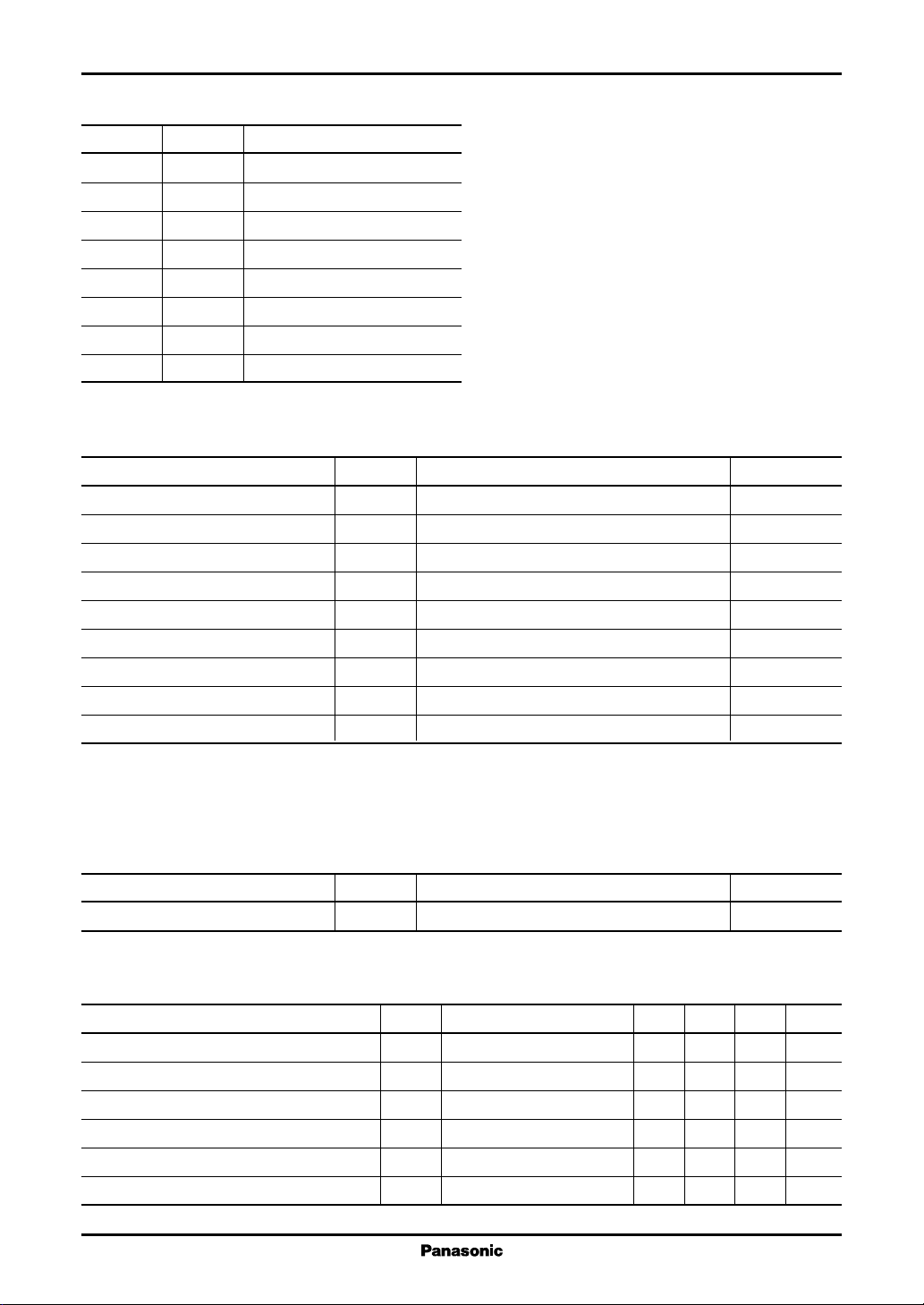
■ Pin Descriptions
Pin No. Symbol Description
1VSReference voltage
2 Stop Oscillation stop input
3 Reset Reset input
4 GND Grounding
5 CR C and R connection
6 Out Output
7VCCSupply voltage
8 Mon. Monitor pin
■ Absolute Maximum Ratings
Parameter Symbol Rating Unit
Supply voltage V
Supply current I
Power dissipation P
Operating ambient temperature
Storage temperature
*
*
Stop terminal voltage V
Reset terminal voltage V
CR terminal voltage V
Out terminal current I
Note) 1. Do not apply external currents or voltages to any pins not specifically mentioned.
For circuit currents, '+' denotes current flowing into the IC, and '−' denotes current flowing out of the IC.
2. *: Except for the operating ambient temperature and storage temperature, all ratings are for Ta = 25°C.
CC
CC
D
T
opr
T
stg
STOP
RESET
CR
OUT
20 V
7mA
140 mW
−35 to +85 °C
−55 to +125 °C
0 to 18 V
0 to 18 V
0 to 3 V
−15 to +15 mA
■ Recommended Operating Range
Parameter Symbol Range Unit
Supply voltage V
CC
■ Electrical Characteristics at Ta = 25°C
Parameter Symbol Conditions Min Typ Max Unit
Quiescent supply current I
Internal reference voltage V
High-level input current I
Low-level input current I
High-level out terminal voltage V
Low-level out terminal voltage V
2
3.2 to 18.0 V
VCC = 5 V 2.0 4.0 5.0 mA
CC
VCC = 5 V, IS = −3 mA 2.40 2.55 2.70 V
S
VCC = 18 V, VIH = 18 V 10 µA
IH
VCC = 18 V, VIL = 0 V −100 µA
IL
VCC = 18 V, IOH = −10 mA 14.0 16.0 18.0 V
OH
VCC = 3.2 V, IOL = −10 mA 0.4 V
OL

ICs for Timer AN6783S
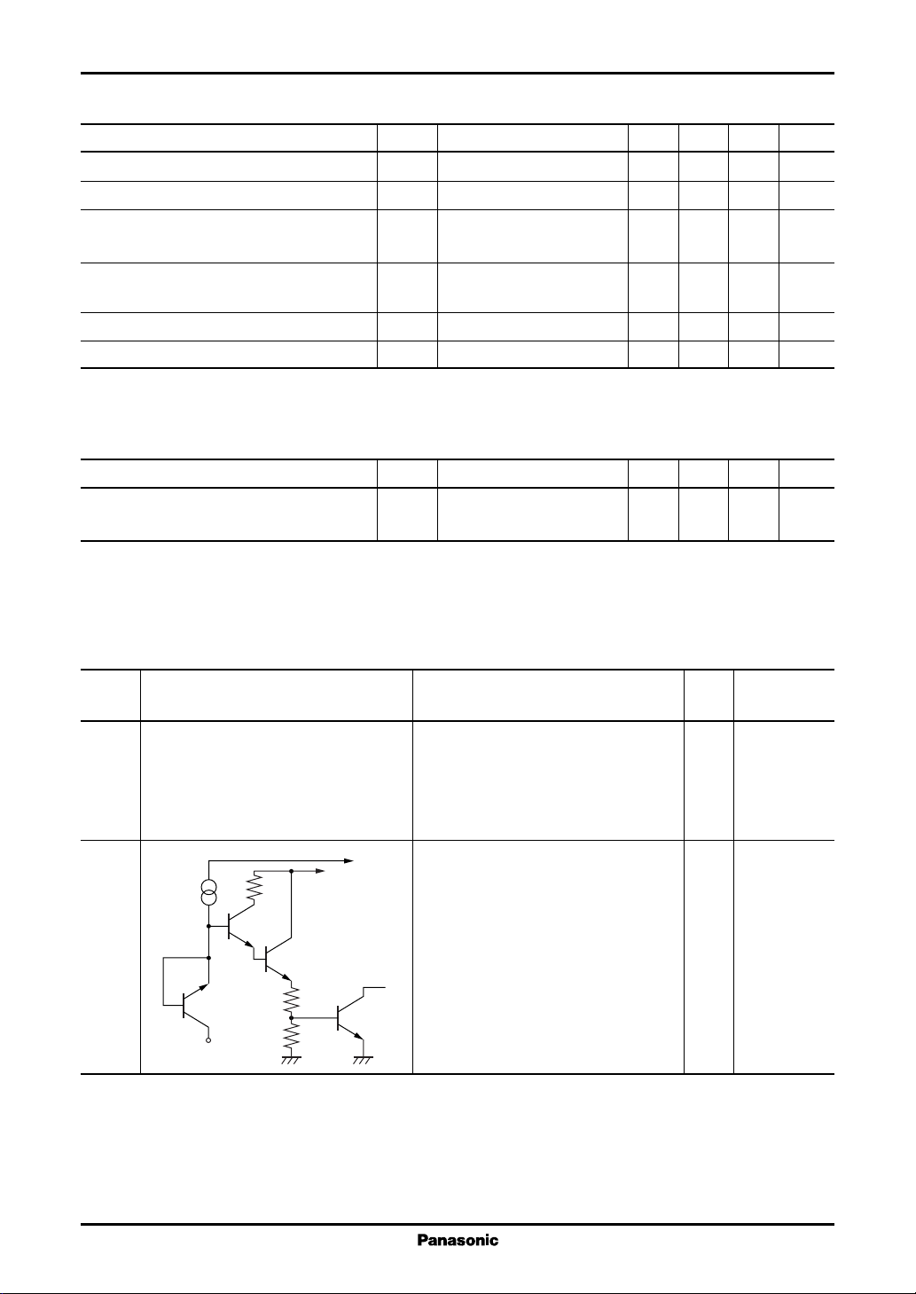
■ Electrical Characteristics at Ta = 25°C (continued)
Parameter Symbol Conditions Min Typ Max Unit
High-level Mon. terminal voltage V
Low-level Mon. terminal voltage V
Oscillation frequency precision f
Oscillation frequency fluctuation with ∆f
supply voltage 3.2 V to 18.0 V
High-level input voltage V
Low-level input voltage V
• Design reference data
Note) The characteristic values below are theoretical values for designing and not guaranteed.
The data show the changing amount within Ta = −35°C to +85°C when the values at Ta = 25°C is taken as the reference.
Parameter Symbol Conditions Min Typ Max Unit
Oscillation frequency- ∆f
temperature dependency CT = 0.1 µF
VCC = 18 V 17.8 18.0 V
MH
VCC = 3.2 V 0.4 V
ML
VCC = 5 V, RT = 1 kΩ, 9.0 9.5 10.0 kHz
OSC
CT = 0.1 µF
VCC = 5 V, −5.0 5.0 %
V
VCC = 5 V 2.0 V
IH
VCC = 5 V 0.8 V
IL
VCC = 5 V, RT = 1 kΩ, −5.0 5.0 %
r
■ Terminal Equivalent Circuits
Pin No. Equivalent circuit Description I/O
1 V
2 Stop : I
V
CC
V
S
Stop
: O 2.55 V
S
Stabilized power supply output terminal.
Reference voltage source for oscillation
circuit.
Oscillation stop input terminal. Only the
oscillation circuit stops when this terminal becomes low-level.
(F.F. is not cleared)
When not used, the terminal should be
open or connected to V
CC
.
DC
voltage
3
 Loading...