

Panasonic AN6721 Datasheet
7
6
5
4
3
2
0.3
+ 0.1
– 0.05
18.2±0.3
6.0±0.3
2.4±0.25
1.5±0.25
0.5±0.1
2.54
1.5±0.25
3.0±0.3
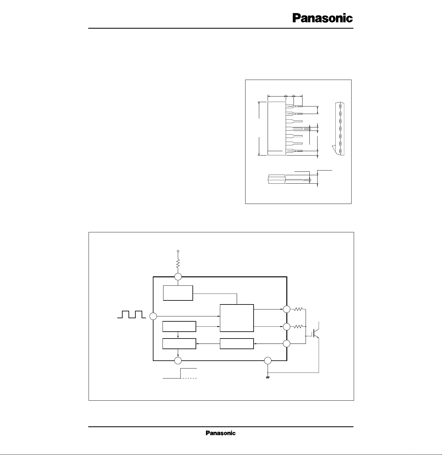
Unit : mm
1
3.5±0.25
7-pin SIP Package (SIP007-P-0000)
30˚
■ Overview
The AN6721is an IC with driver which drives the IGBT of large
power element and various protective functions. It is suitable for
drive of IH jar rice cooker or electromagnetic cooker.
■ Features
•
Turning-on and -off driving capabilities of power element
able to be set separately
•
Shunt regulator circuit built-in
•
Low VCCprotection function built-in
•
Power-on protective function built-in.
At power-on, the output is fixed to “Low” until the VCCrises
to protect the power element from mis-conduction.
•
Protective operation signal output
It transmits the signal to the control side when any of the abo-
ve protective functions are activated.
AN6721
IGBT Drive IC
7
1
2 4
6
5
3
V
CC
IN
0V
5V
Q
1
ONOFF
OPEN
LOW
V
DD
OUT (H)
OUT (L)
PRT
GND
Q
1
IGBT
Regurator
Driver
Switch on ProtectorProtection Signal
■ Block Diagram
Low V
CC Protector
Protector
Operating Normal
Po
■ Pin Name
Pin No.
Pin name
1
2
3
4
5
6
7
Input terminal (IN)
Protection operation signal output terminal (PO)
Power-on protection terminal (PRT)
GND
Output (L) terminal (OUT (L))
Output (H) terminal (OUT (H))
V
CC
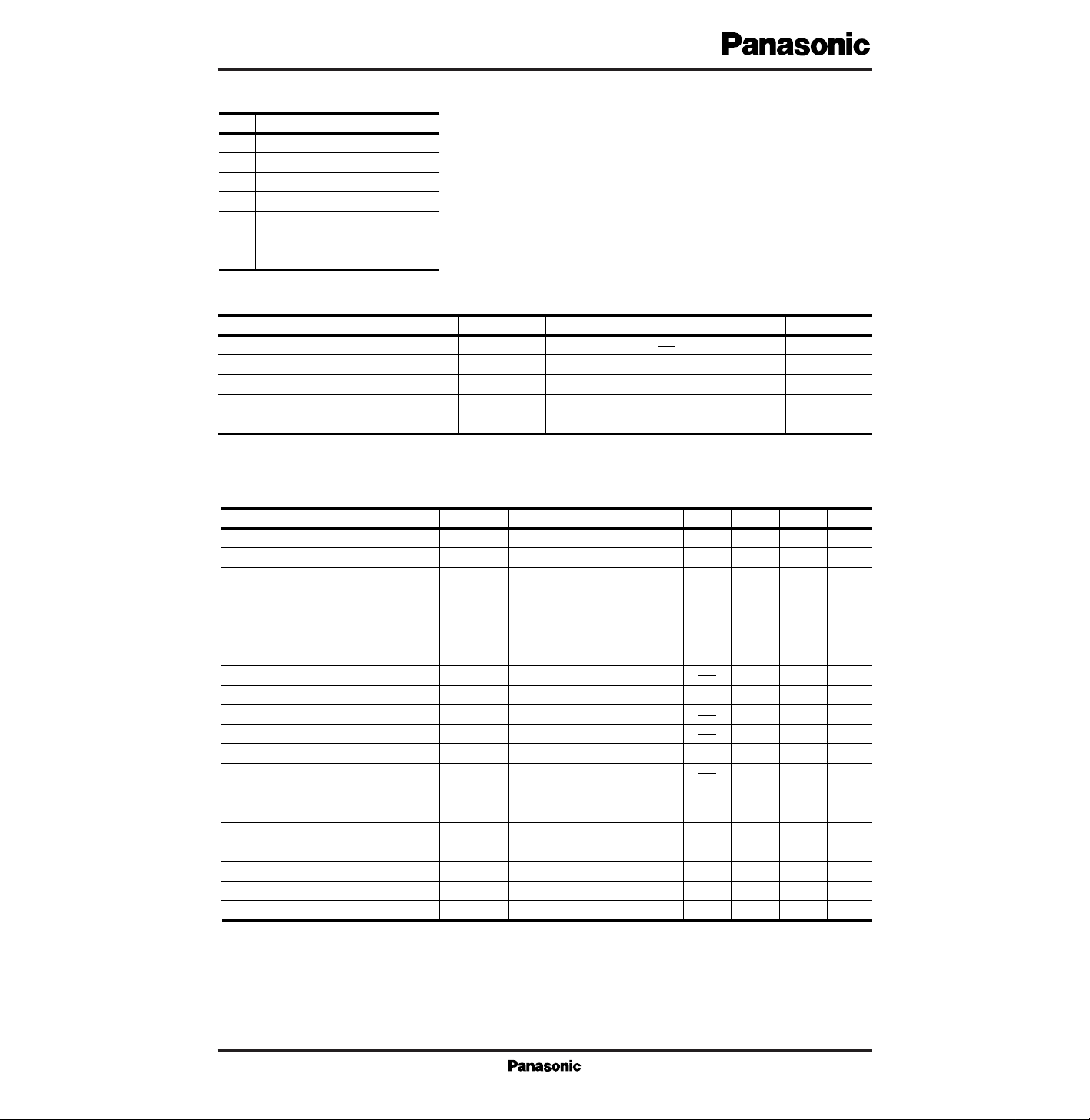
Parameter Symbol Rating Unit
■ Absolute Maximum Rating (Ta=25˚C)
Supply voltage
Note 1)
Supply current
Note 2)
Power dissipation
Note 2)
Operating ambient temperature
Storage temperature
V
CC
I
CC
P
D
T
opr
T
stg
21
525
–20 to 85
–55 to 150
V
mA
mW
˚C
˚C
Note 1) The supply voltage value is limited by shunt regulator.
Note 2) Under Ta=85˚C
Parameter Symbol Condition min typ max Unit
■ Electrical Characteristics (Ta=25±2˚C)
Supply current (1)
Supply current (2)
Regulator voltage (1)
Regulator voltage (2)
Low V
CC
protection threshold
Low VCC protection threshold difference
Low VCC protection lower limit
Low V
CC
protection upper limit
Power-On protection threshold
Power-On protection voltage
Protection operation signal output
Output voltage (H)
Output voltage (L)
Output voltage (L)
Input voltage threshold
Input voltage threshold difference
Sink current peak value
Source current peak value
Fall time lag
Rise time lag
I
CC1
I
CC2
V
CC (R) 1
V
CC (R) 2
V
VL
DV
V
V
CC (L)
V
OL
V
P
V
PRT
V
PO
V
OH
V
OL1
V
OL2
V
IL
DV
I
I
f
I
r
t
df
t
dr
VCC=20V
V
CC
=20V
I
CC
=6mA
I
CC
=21mA
V
1
=5V
V
1
=5V
V
1
=5V
I
O
=30mA
V
3
=4V
I
PRT
=30mA VCC=1V
I
PO
=0.5mA VCC=1V
I
O
=–5mA
I
O
=100mA
I
O
=30mA
V
CC
=38V
V
CC
=38V
R
O
=10Ω CO=18000pF
R
O
=10Ω CO=6800pF
R
H
=4.3kΩ RL=200Ω
R
H
=4.3kΩ RL=200Ω
2.1
7
21.3
21.4
9.5
0.55
6.5
20.5
1.75
0.35
1.05
0.45
0.05
0.3
3.3
8.5
22.7
22.8
9.9
0.61
0.1
7.1
0.8
0.8
22
0.4
0.1
2.05
0.45
1.3
0.6
0.25
0.5
4.5
10
24.1
24.2
10.3
0.67
2.5
0.3
7.7
0.93
0.93
23.5
0.7
0.3
2.35
0.55
0.45
0.7
mA
mA
V
V
V
V
V
V
V
V
V
V
V
V
V
V
A
A
µS
µS
 Loading...