

Panasonic AN6564NS, AN6564, AN1324NS, AN1324 Datasheet
AN1324 (AN6564),
AN1324NS (AN6564NS)
Quadruple Operational Amplifiers
■ Overview
The AN1324 (AN6564)and the AN1324NS
(AN6564NS)are quadruple operational amplifiers with
phase compensation circuits built-in, and with wide range
of operating voltages, allowing single power supply
operation. They have electrical characteristics equal to
the conventional operational amplifiers, and are low
powered and suitable for application to various circuits.
■ Features
• Built-in phase compensation circuit
• Wide range of common-mode input voltage
0V to VCC–1.5V
• Wide range of operating voltages
Single supply:3 to 30V
Dual supply:±1.5 to 15V
1
2
3
4
5
19.06±0.3
6
7
6.35±0.3
3–15˚
7.62±0.25
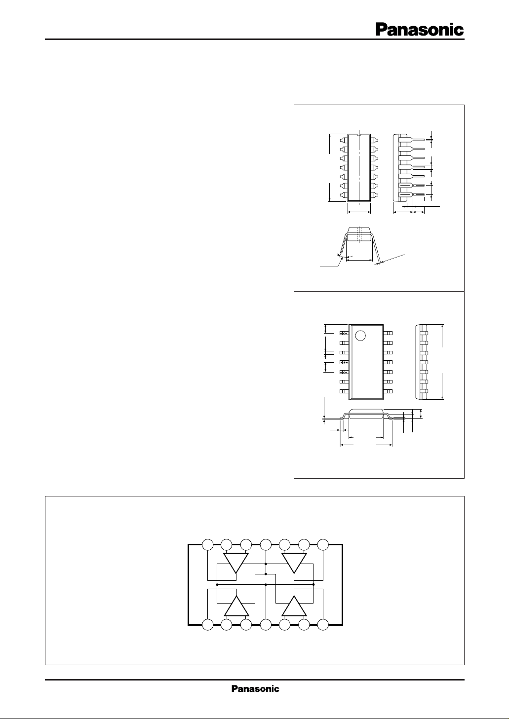
14-pin DIL Plastic Package (DIP014-P-0300D)
1.24
1
2
3
0.4±0.25
4
1.27
5
6
7
14
13
12
11
10
9
8
0.3
+0.1
1.1±0.25
3.05±0.254.7±0.25
– 0.05
14
13
12
11
10
9
8
Unit :mmAN1324 (AN6564)
0.5±0.11.22±0.25
2.54
Unit:mmAN1324NS (AN6564NS)
10.1±0.3
■ Block Diagram
0.1±0.1
14-pin PANAFLAT Plastic Package (SOP014-P-0225A)
GND
+
–
V
V
in4
O4
14
13 12 11
–
–
1 234567
V
V
in1
O1
(VEE)V
in4
+
4
1
+
+
–
V
in1
V
CC
+
V
V
–
V
in3
in3
10 9 8
+
–
3
2
–
+
–
+
V
in2
in2
V
O3
V
O2
0.3
4.2±0.3
6.5±0.3
0.15
1.5±0.2
0.45
■ Pin Descriptions
Pin No.
1
Ch.1 output
2
Ch.1 inverting input
3
Ch.1 non inverting input
4
V
CC
Ch.2 non inverting input
5
Ch.2 inverting input
6
Ch.2 output
7
Pin name Pin name
Pin No.
8
Ch.3 output
9
Ch.3 inverting input
10
Ch.3 non inverting input
11
GND (V
Ch.4 non inverting input
12
Ch.4 inverting input
13
Ch.4 output
14
■ Absolute Maximum Ratings (Ta=25˚C)
Parameter Symbol Rating Unit
Supply voltage
Voltage
Power dissipation
Operating ambient temperature
Storage temperature
Differential input voltage
Common-mode input voltage
Output voltage
AN1324 (AN6564)
AN1324NS (AN6564NS)
AN1324 (AN6564)
AN1324NS (AN6564NS)
)
EE
V
CC
V
ID
V
ICM
V
O
P
D
T
opr
T
stg
32
32
–0.3 to 32
24
570
380
–20 to +75
–55 to +150
–55 to +125
V
V
V
V
mW
˚C
˚C
■ Electrical Characteristics (VCC=5V, Ta=25˚C)
Parameter Symbol Condition min typ max Unit
Input offset voltage
Input bias current
Input offset current
Common-mode input voltage range
Supply current
Voltage gain
Maximum output voltage
Common-mode rejection ratio
Supply voltage rejection ratio
Channel separation
Output source current
Output sink current
V
I (offset)
I
Bias
I
IO
CM
I
CC
G
V
V
O(max.)
CS dB120
I
O(source)
I
SINK
=50Ω
R
S
=∞
R
L
≥2kΩ
R
L
=2kΩ
R
L
f=1kHz to 20kHz
+
=1V, V
V
in
+
=0V, V
V
in
7mV2
500 nA
50 nA
0V
VCC–1.5
V
mA
2
dB100
VCC–1.5
V
65CMR dB85
65SVR dB100
–
=0V
in
–
=1V
in
20
10
mA40
mA20
 Loading...