

Panasonic AN6551 Datasheet
AN6551
Dual Operational Amplifier
■ Overview
The AN6551 is a dual operational Amplifier with a phase
compensation circuit built-in.
It is suitable for application to various electronic circuits
such as active filters and audio pre-amplifiers.
■ Features
• Phase compensation circuit
• High gain, low noise
• Output short-circuit protection
• T w o circuits symmetrically arranged in 9-pin SIL plastic
package
■ Pin Descriptions
Pin No.
2
Ch.1 output
3
Ch.1 inverting input
4
Ch.1 non inverting input
5
V
Ch.2 non inverting input
6
Ch.2 inverting input
7
Ch.2 output
8
V
1, 9
(GND)
EE
CC
Pin name
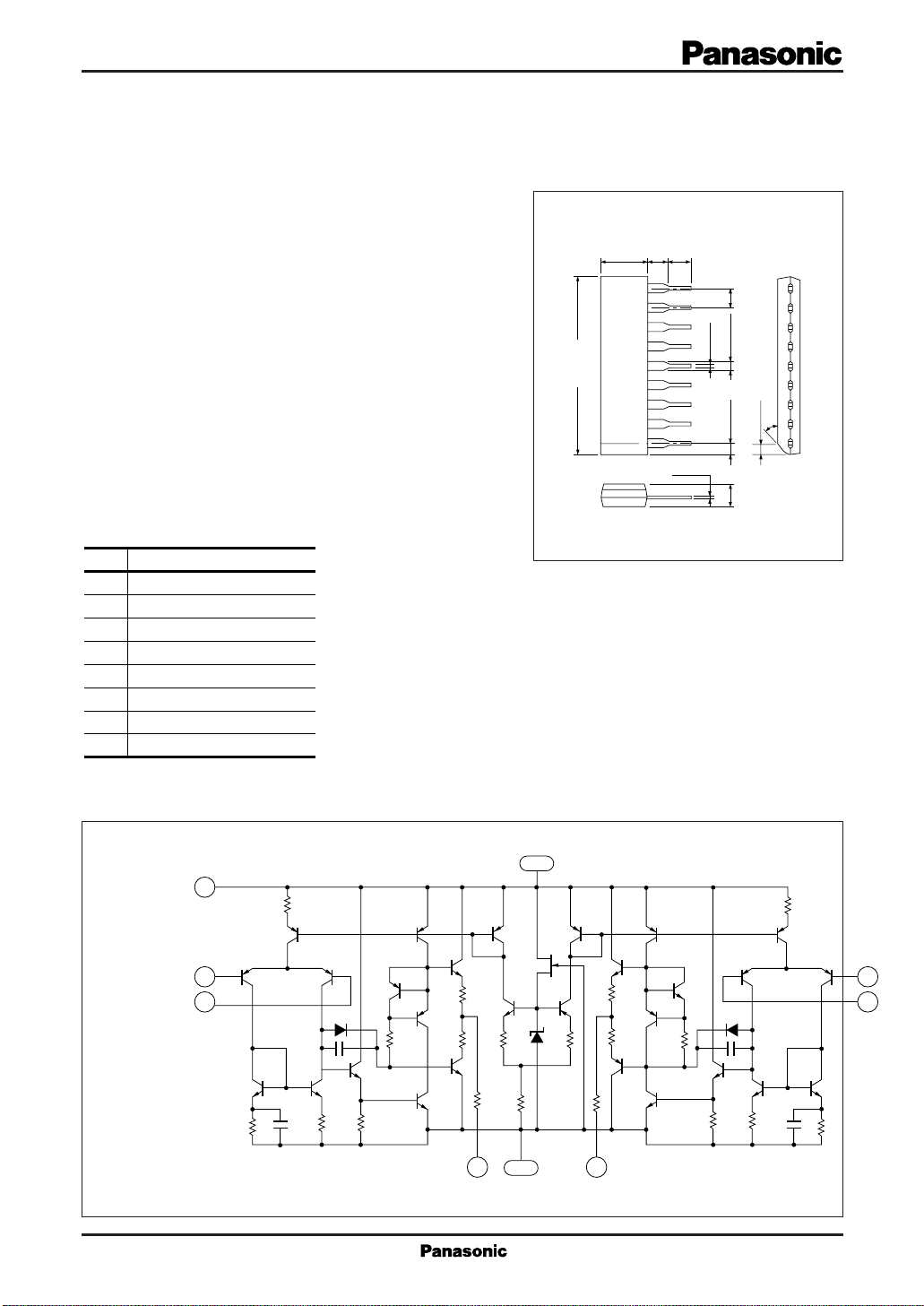
2.4±0.25
6.0±0.3
3.3±0.25
9
8
2.54
7
6
23.3±0.3
5
4
1.5±0.25
0.5±0.1
3
2
1
1.5±0.25
+0.1
0.3
– 0.05
3.0±0.3
9-pin SIL Plastic Package (SIP009-P-0000C)
Unit:mm
30˚
1.4±0.3
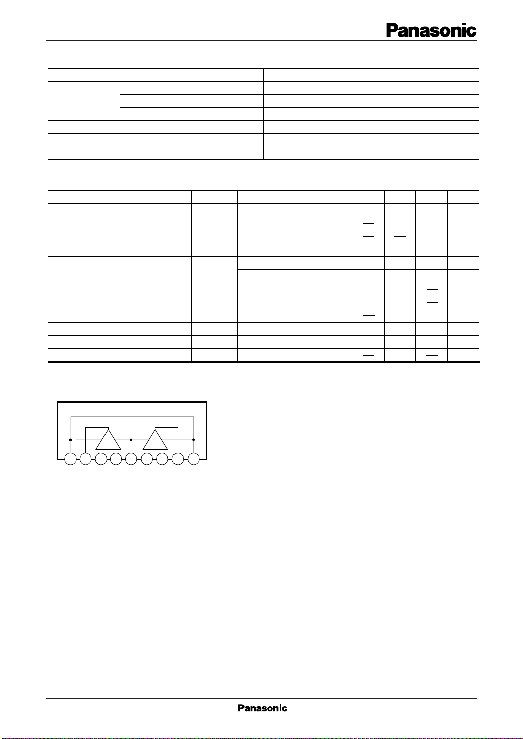
■ Block Diagram
V
CC
1
V
3
4
V
V
CC
9
R
3
Q
Q
–
in1
+
in1
3
Q
Q
4
R
1
Q
1
2
Q
5
C
1
D
1
C
2
R2R
Q
Q
6
4
10
Q
11
8
R
6
Q
Q
9
R
5
Q
7
14
R
12
R
7
Q
12
R
8
2 8
V
VEE (GND)
O1
Q
Q
28
13
Q
15
Q
D
Z
R
13
R
9
5
Q
25
Q
26
Q
R
19
29
Q
R
20
Q
27
21
R
Q
V
O2
23
D
24
R
18
22
2
C
4
Q
21
Q
R
R
17
R
16
Q
18
Q
20
15
Q
17
16
Q
19
C
3
R
14
–
V
7
in2
+
6
V
in2
■ Absolute Maximum Ratings (Ta=25˚C)
Parameter Symbol Rating Unit
VCC, V
V
V
ICM
P
T
opr
T
stg
EE
ID
D
Voltage
Power dissipation
Temperature
Supply voltage
Differential input voltage
Common-mode input voltage
Operating ambient temperature
Storage temperature
■ Electrical Characteristics (VCC=15V, VEE=–15V, Ta=25˚C)
Parameter Symbol Condition min typ max
Input offset voltage
Input offset current
Input bias current
Voltage gain
Maximum output voltage
Common-mode input voltage width
Common-mode rejection ratio
Supply voltage rejection ratio
Power consumption
Slew rate
Equivalent input noise voltage
V
I (offset)
I
IO
I
bias
V
V
O (max.)
CM
SVR µV/V30
P
C
SR V/µs1.0
V
ni
<
10kΩ
R
S
=
>
2kΩ, VO=±10V
R
L
=
>
R
10kΩ
L
=
>
R
2kΩ
L
=
=∞
R
L
>
R
2kΩ
L
=
=1kΩ, B=10Hz to 30kHz
R
S
±18
±30
±15
500
–20 to +75
–55 to +150
86G
100
±12
±10 V±13
±12V
70CMR dB90
V
V
V
mW
˚C
˚C
Unit
6mV0.5
200 nA5
500 nA
dB
V±14
V±14
150
170 mW90
µVrms2.5
■ Block Diagram
+
–
1 23456 879
V
CC
V
O1
–
V
V
in1
+
in1VEE
+
–
–
+
V
V
in2
in2
V
CCVO2
 Loading...