

Panasonic AN6472NFBP Datasheet
1
ICs for Telephone
■ Overview
The AN6472NFBP is a speech network IC which
includes a receiver noise reducing function and is most
suitable for quality cordless telephones. It incorporates a
cross-point switch controlled by serial input. It allows
speech path switching and mixing, and provides for
three- or four-person communication and other sophisticated functions. It also incorporates REC/PLAY amplifiers
with VOX circuits.
■ Features
•
The speech block can operate on line voltage, with no
external power supply, and is operational even during a
commercial power failure.
•
Incorporates a receiver noise reducing function to
improve the handset's howling margin.
•
Incorporates auto. PAD, dial mute, DC voltage regulation, and other basic speech functions.
•
The cross-point switch can be operated independently.
•
Each output of the cross-point switch can correspond to
multiple inputs, allowing three- or four-person communication.
•
The REC/PLAY amplifiers incorporate ALC and VOX
circuits.
•
Receiver volume can be increased by 6 dB or 9 dB.
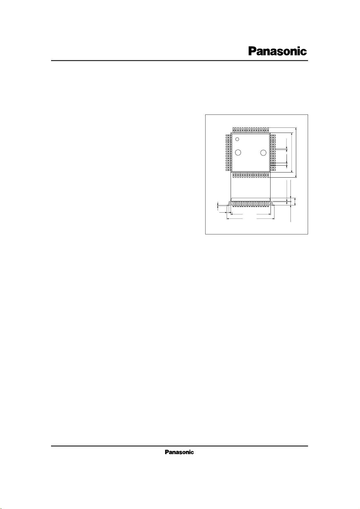
AN6472NFBP
Cordless Telephone Speech Network IC Incorporating
Cross-Point Switch
1
16
0.35±0.1
0.1±0.1
0.55
1.3±0.25
2.8±0.2
14.0±0.3
17.2±0.4
QFP package with 64 pins (QFH064-P-1414)
Unit : mm
0.15
1.3±0.25
0.8
14.0±0.3
17.2±0.4
17 32
64
48
33
49
+0.1
–0.05
2
ICs for Telephone
AN6472NFBP
1 2 3 4 5 6 7 8 9 10 11 12 13 14 15 16
64
63
62
61
60
59
58
57
56
55
54
53
52
51
50
49
48 47 46 45 44 43 42 41 40 39 38 37 36 35 34 33
32
31
30
29
28
27
26
25
24
23
22
21
20
19
18
17
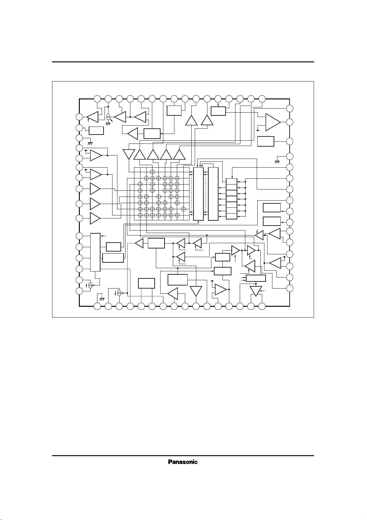
–
+
–
+
6dB
0dB
0dB
Det.
30dB
AP
Control
AP
0dB
0dB
V
REF
0dB
+–
AP
DMC
DMC VCC
0/6/9dB
L(27)
L(
17)
L(1F)
0dB
DMC
DMC
0dB
0dB
L(OF)
VCC
+–
+–
L(3F)
DC
Control
DM
Control
+
–
V
REF
+
–
L(07)
ALC
Det.
0dB
0dB
VOX
Det.
Noise
Protection
Decoder
Latch
Power Supply
Control
INJ
P.O.R
Line Supply
Monitor
D
a1
a2
a3
a4
a5
a6
COMP
ALC
10dB
0dB
0dB
0/12
dB
20
dB
18dB18
dB
DCC
GND
GND
GND
■ Block Diagram
3
ICs for Telephone
AN6472NFBP
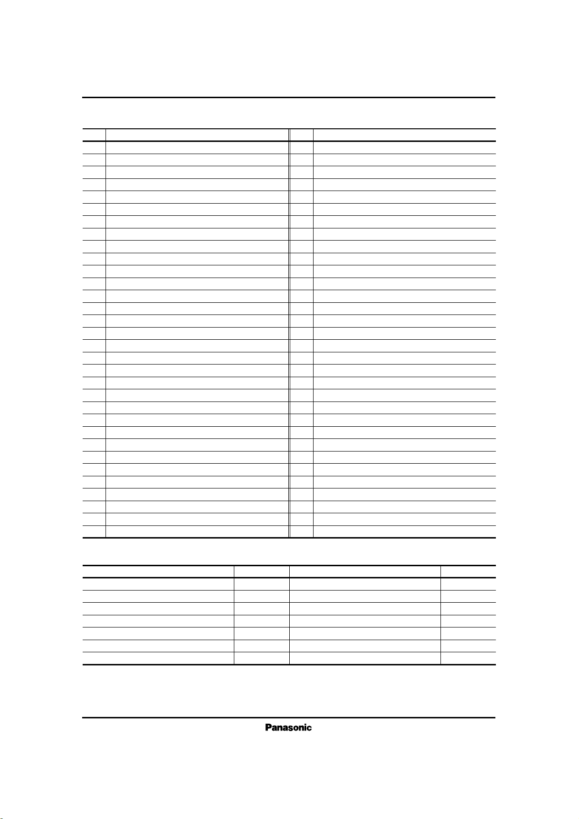
■ Pin Descriptions
Pin No.
Description
1
2
3
4
5
6
7
8
9
10
11
12
13
14
15
16
17
18
19
20
21
22
23
24
25
26
27
28
29
30
31
32
Ground
Line power (+) input
Side-tone adjustment
Line voltage control (1)
Int. ref. voltage output (2)
Int. ref. voltage output (1)
Trans. preamp. output
Noise reduction detection output
Noise reduction detection input
Noise reduction amp. output
Auto. PAD control
Rec. preamp. input
Rec. preamp. output
Rec. amp. input
Rec. amp. output (1)
Rec. amp. output (2)
BT signal input
DTMF preamp. output
DTMF signal input
MIC preamp. output
MIC preamp. input (1)
MIC preamp. input (2)
Dial mute control
Line voltage control
Line interruption detector output
Strobe signal input
Clock signal input
Data input
Ground
Logic power supply input
VOX detector output
SP link output
Pin No.
Description
33
34
35
36
37
38
39
40
41
42
43
44
45
46
47
48
49
50
51
52
53
54
55
56
57
58
59
60
61
62
63
64
RF2 link output
RF1 link output
Intercom link output
VOX detection control
VOX amp. input
Time stamp link output
Recording link output
ALC input
ALC detection control
Loudspeaker link input
Recording input
Recording inverse input
Recording preamp. output
Recording bias current control
To recording head
EQ amp. inverse input
EQ amp. output
REC/PLAY int. ref. voltage output
Ground
MIX preamp. output
MIX link input
AUX preamp. output
AUX link input
Intercom link input
RF1 link input
RF2 link input
Power-ON reset control
External supply voltage input
Internal supply voltage output
Circuit voltage control (2)
Line current bypass (2)
Line current bypass (1)
*1 In a free-air condition with Ta=75˚C
V
CC
I
CC
V
L
I
L
P
D
T
opr
T
stg
Supply voltage (1)
Supply current (1)
Supply voltage (2)
Supply current (2)
Power dissipation*1
Operating ambient temperature
Storage temperature
V
mA
V
mA
mW
˚C
˚C
Parameter Symbol Rating Unit
■ Absolute Maximum Ratings (Ta=25˚C)
7.0
50
12.0
135
640
–20 to+75
–55 to+150
4
ICs for Telephone
AN6472NFBP
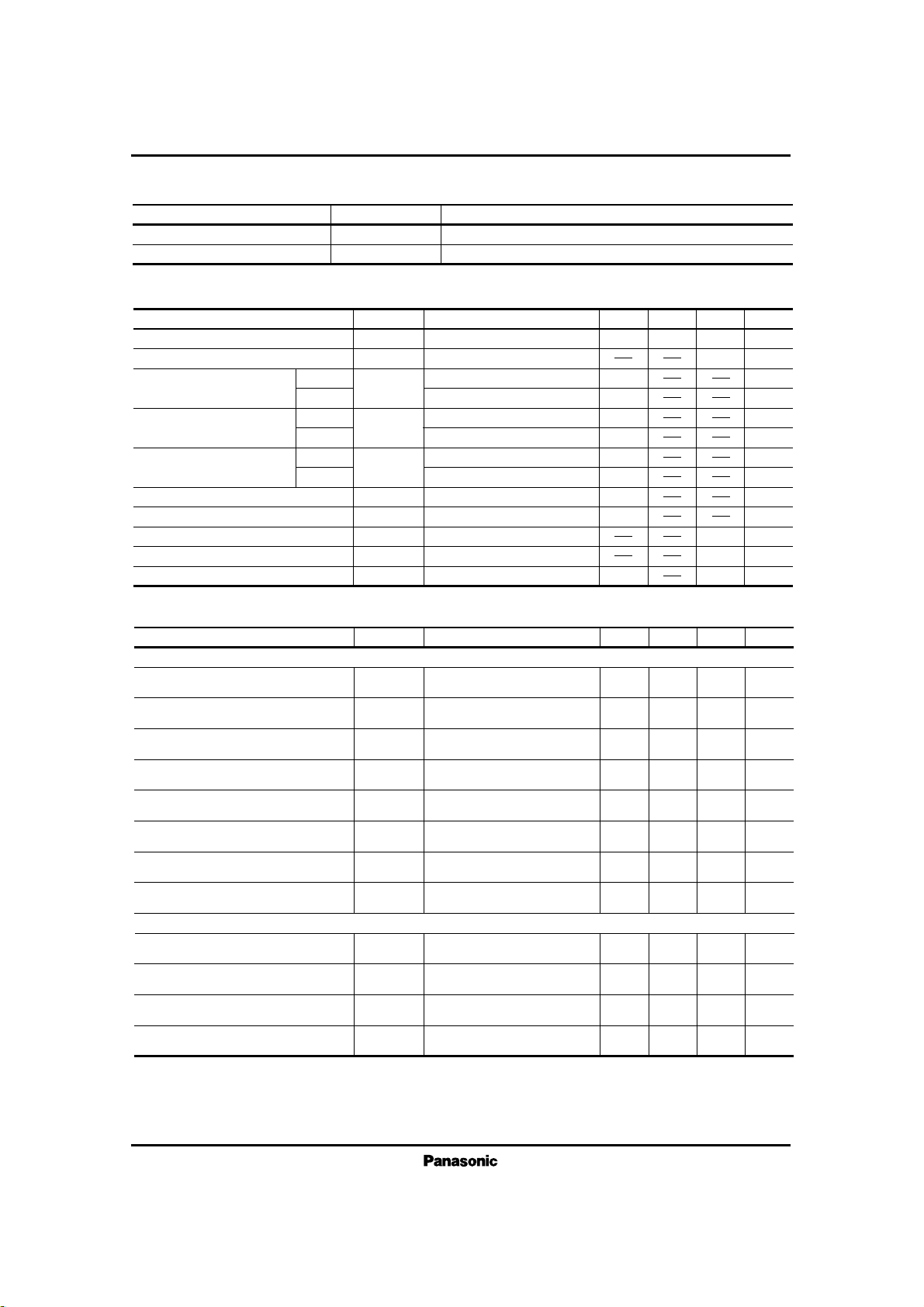
Parameter Symbol Range
■ Recommended Operating Range
Operating supply voltage range (1)
Operating supply voltage range (2)
V
CC
V
L
4.5V to 5.5V
3.0V to 11.0V
Parameter Symbol min
4.5
1.6
1.2
1.6
0.8
1.6
1.2
0.8
0.8
0
5 5.5
250
20
20
V
CC
V
kHz
µs
µs
µs
µs
µs
µs
µs
µs
µs
µs
V
typ max Unit Condition
■ Recommended Operating Conditions (Ta =20 to +75˚C)
Supply voltage
Clock frequency
Input pulse width (high)
Input pulse width (low)
Clock pulse rise time
Clock pulse fall time
Input voltage
Input pulse width
Setup time
Hold time
V
CC
f
CLK
Input Duty 40% to 50%
t
W
t
su
t
h
t
wh
t
wl
t
r
t
r
V
i
CLK
STB
DATA
STB
DATA
STB
Parameter Symbol Condition min typ max
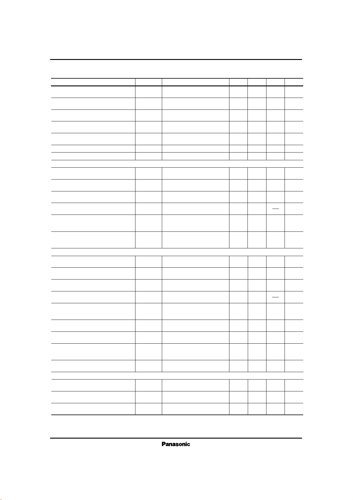
■ Electrical Characteristics (Ta=25±2˚C)
Power Supply Characteristics During Power Failure
Normal power supply characteristics
Line DC voltage (I-1)
V
L – I1
V3.5 3.83.2
Unit
V–DCC=HIGH,
IL=20mA, VCC=0V
Line DC voltage (E-1)
V
L – E1
V3.4 3.83.1
V– DCC=HIGH,
IL=20mA, VCC=5V
Line DC voltage (E-2)
V
L – E2
V4.7 5.14.3
V–DCC=HIGH,
IL=20mA, VCC=5V
V
L – E3
V6.8 7.36.3
V–DCC=HIGH,
IL=20mA, VCC=5V
Line DC voltage H (E-1)
V
LH – E1
V4.85 5.44.3
V–DCC=HIGH,
IL=20mA, VCC=5V
Line DC voltage (I-2)
V
L – I2
V4.8 5.24.5
V–DCC=HIGH,
IL=60mA, VCC= 0V
Line DC voltage (I-3)
V
L – I3
V7.0 7.56.6
V–DCC=HIGH,
IL=120mA, VCC= 0V
Line DC voltage H (I-1)
V
LH – I1
V5.0 5.54.5
V–DCC= LOW,
IL=30mA, VCC= 0V
Line DC voltage H (I-2)
V
LH – I2
V6.2 6.75.7
V–DCC= LOW,
IL= 60mA, VCC= 0V
Line DC voltage H (I-3)
V
LH – I3
V8.5 9.27.9
V–DCC= LOW,
IL=120mA, VCC= 0V
Internal supply voltage (I)
V
reg – I
V2.0 2.21.8
V– DCC=HIGH,
IL=20mA, VCC= 0V
Internal ref. supply voltage (I)
V
ref – I
V1.0 1.10.9
V–DCC=HIGH,
IL=20mA, VCC= 0V
Line DC voltage (E-3)
5
ICs for Telephone
AN6472NFBP
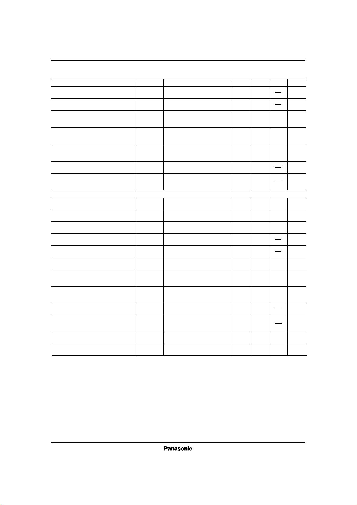
Parameter Symbol Condition min typ max
■ Electrical Characteristics (cont.) (Ta=25±2˚C)
Receiver During Power Failure
Line DC voltage H (E-2)
V
LH – E2
V5.95 6.65.3
Unit
V–DCC=LOW,
I
L
=60mA, VCC=5V
Rec. gain (I-1)
G
V – IR1
dB32.5 34.530.5
IL=30mA, VCC= 0V
Vin= – 42dBm
Rec. gain (I-2)
G
V – IR2
dB29 3127
IL= 80mA, VCC= 0V
Vin= –42dBm
Rec. auto. PAD width (I)*1
A
P – IR
dB3.5 52.5
IL=30mA– 80mA, VCC= 0V,
Vin= – 42dBm
Rec. max. output (I)
Rec. noise reduction (I)
V
O – IR
N
L – IR
dBm40
4
19
6
21
8
23
dB
dB
With IL=30mA, VCC= 0V, and
THD=5%
I
L
=30mA, VCC= 0V,
Vin= –42dBm
Vin–M= –65/–50dBm
I
L
=30mA, VCC= 0V,
V–DMC=LOW,
Vin= –30dBm
Line DC voltage H (E-3)
V
LH – E3
V8.2 8.97.55
V–DCC=LOW,
IL=120mA, VCC=5V
Internal supply voltage (E)
V
reg – E
V4.85 5.04.6
V–DCC=HIGH,
IL=20mA, VCC=5V
Internal ref. supply voltage (E)
V
ref – E
V2.5 2.72.25
V–DCC=HIGH,
IL=20mA, VCC=5V
Total circuit current
Power interruption detection (1)
Power interruption detection (2)
I
total
V
– HIT1
V
– HIT2
mA27 3517
0
4.4
0.1
4.95
0.6
5
V
V
V–DCC=HIGH,
IL=20mA, VCC=5V
VL=2.7V, VCC=5V
V
L
=1.5V, VCC=5V
G
V – IBT
Receiver On External Power Supply
Transmitter Amp. During Power Failure
Rec. gain (E-1)
G
V – ER1
dB32.5 34.530.5
IL=30mA, VCC=5V
Vin= –42dBm
Trans. gain (I-1)
G
V – IM1
dB30.2 32.228.2
R=27Ω(Pin3), IL=30mA,
VCC=0V, Vin= –38dBm
Trans. gain (I-2)
G
V – IM2
dB26.4 28.424.4
IL=80mA, VCC=0V,
Vin= –38dBm
A
P – IM
dB3.8 52.5
IL=30mA–80mA, VCC=0V,
Vin= –38dBm
Rec. gain (E-2)
G
V – ER2
dB28.8 30.826.8
IL=30mA, VCC=5V
Vin= –42dBm
Rec. auto. PAD width (E)*1
A
P – ER
dB3.7 52.5
IL=30mA–80mA, VCC=5V
Vin= –42dBm
Rec. max. output (E)
V
O – ER
dBm124
With IL=30mA, VCC=5V, and
THD=5%
Rec. noise reduction (E)
N
L – ER
dB8106
IL=30mA, VCC=5V,
Vin= –42dBm
Vin–M= –65/–65dBm
Rec. digital volume (1)*2
G
V – DV1
dB675
IL=30mA, VCC=5V,
V
in
= –42dBm, DV–1 ON
Rec. digital volume (2)*2
G
V – DV2
dB9 10.57.5
IL=30mA, VCC=5V,
Vin= –42dBm, DV–2 ON
BT amp. gain (E)
G
V – EBT
dB21.5 23.519.5
I
L
=30mA, VCC=5V,
V–DMC=LOW,
Vin= –30dBm
Rec. gain difference
DG–R dB– 0.1 1.2–1.2
For V
CC
=0V and 5V(between
Gv–IR1 and Gv–ER1)
BT amp. gain (I)
Trans. auto. PAD width (I)*1
Note) Unless otherwise specified, input signal Fin =1kHz, control voltage V-DOC = high, and control voltage V-DMC = high.
*1 Gain decrease when line current I
L
is changed from 30 to 80 mA. If pin 11 (auto. PAD control)is connected to pin 61 (int.
supply voltage output), the gain will not change.
*2 Gain increase from receiver gain (E-1).
6
ICs for Telephone
AN6472NFBP
Parameter Symbol Condition min typ max
■ Electrical Characteristics (cont.) (Ta=25±2˚C)
Transmitter Amp. On External Power Supply
Trans. max. output (I-1)
V
O – IM1
dBm3.50
Unit
With I
L
=30mA, VCC= 0V and
HD=5%
DTMF max. output (I-1)
V
O – ID1
dBm3.80
IL=30mA, VCC=0V,
V–DMC=LOW, THD=5%
Trans. gain (E-1)
G
V – EM1
dB30.6 32.628.6
IL=30mA, VCC= 0V,
Vin= –38dBm
Trans. gain (E-2)
G
V – EM2
dB27.0 29.025.0
IL=80mA, VCC=5V,
Vin= –38dBm
Trans. auto. PAD width (E)*1
A
P – EM
dB452.5
IL=30mA–80mA, VCC=5V,
Vin= –38dBm
Trans. max. output (E-1)
V
O – EM1
dBm62
With IL=30mA, VCC=5V and
THD=5%
Trans. max. output (E-2)
V
O – EM2
dBm62
IL=30mA, VCC=5V,
THD=5%, V–DCC=LOW
Trans. max. output (I-2)
V
O – IM2
dBm3.50
With IL=30mA, VCC= 0V,
THD=5% and V–DCC=LOW
DTMF gain (I-1)
G
V – ID1
dB19.5 21.517.5
IL=30mA, VCC= 0V,
V–DMC= LOW,
Vin= –30dBm
DTMF gain (I-2)
G
V – ID2
dB15.7 17.713.7
IL=80mA, VCC= 0V,
V–DMC=LOW,
V
in
= –30dBm
DTMF max. output (I-2)
V
O – ID2
dBm3.50
IL=30mA, VCC= 0V,
THD=5%, V–DMC=LOW,
V–DCC=LOW
DTMF auto. PAD width (I)*1
A
P – IDT
dB3.8 52.5
IL=30mA–80mA, VCC= 0V,
V–DMC= LOW,
Vin= –30dBm
DTMF gain (E-1)
G
V – ED1
dB20.1 22.118.1
IL=30mA, VCC=5V,
DM=ON, Vin= –30dBm
DTMF max. output (E-1)
V
O – ED1
V
O – ED2
dBm62
IL=30mA, VCC=5V,
V–DMC=LOW, THD=5%
Trans. gain difference
DG – M dB–0.8 0.7–1.8
For V
CC
= 0V and VCC=5V
(between Gv–IM1 and Gv–EM1)
DTMF gain difference
DG – MF dB–1.3 0.2–2.3
For V
CC
= 0V and 5V
(between Gv–ID1 and Gv–ED1)
DTMF gain (E-2)
G
V – ED2
dB16.5 18.514.5
I
L
=80mA, VCC=5V,
V–DMC=LOW,
Vin= –30dBm
DTMF auto. PAD width (E)*1
A
P – EDT
dB4.1 5.52.5
IL=30mA–80mA, VCC=5V,
V–DMC=LOW,
Vin= –30dBm
DTMF max. output (E-2)
dBm62
I
L
=30mA, VCC=5V,
DM=ON, V–DMC=LOW,
THD=5%
Note) Unless otherwise specified, input signal Fin=1 kHz, control voltage V-DOC=high, and control voltage V-DMC=high.
*1 Gain decrease when line current IL is changed from 30 to 80 mA. If pin 11 (auto. PAD control) is connected to pin 61(int.
supply voltage output) , the gain will not change.
 Loading...