

Panasonic AN6426NK Datasheet
1
ICs for Telephone
■ Overview
The AN6426NK incorporates both speech network and
hands-free functions. Its well designed block configuration allows realization of a hands-free telephone with a
minimal number of components.
■ Features
• Incorporates all the functions required of a hands-free
telephone.
• Incorporates all the functions required of a handset.
• Complies with AC and DC impedance requirements.
• Provides a wide dynamic range.
• A noise detecting circuit prevents inadvertent transmis-
sion.
• Operation on an external power supply is available.
• Each mode can be easily controlled.
• A built-in loudspeaker amplifier can operated either on
line voltage or an external power supply.
AN6426NK
Hands-free Speech Network IC
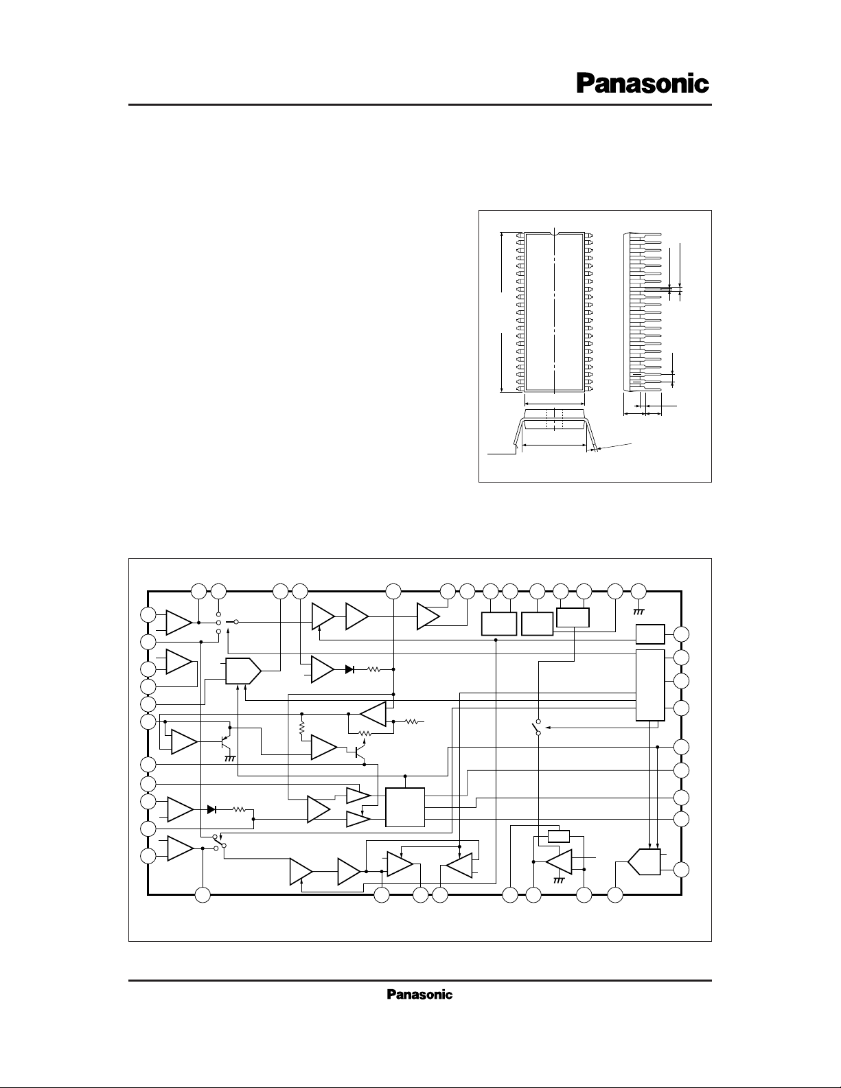
Unit : mm
SDIP package with 42 pins (SDIP042-P-0600A)
3 to 15°
15.3±0.25
0.3
+0.1
– 0.05
13.7±0.3
36.8±0.3
1
21
42
22
0.9±0.25
0.5±0.1
4.76±0.25
4.5±0.25
0.96±0.25
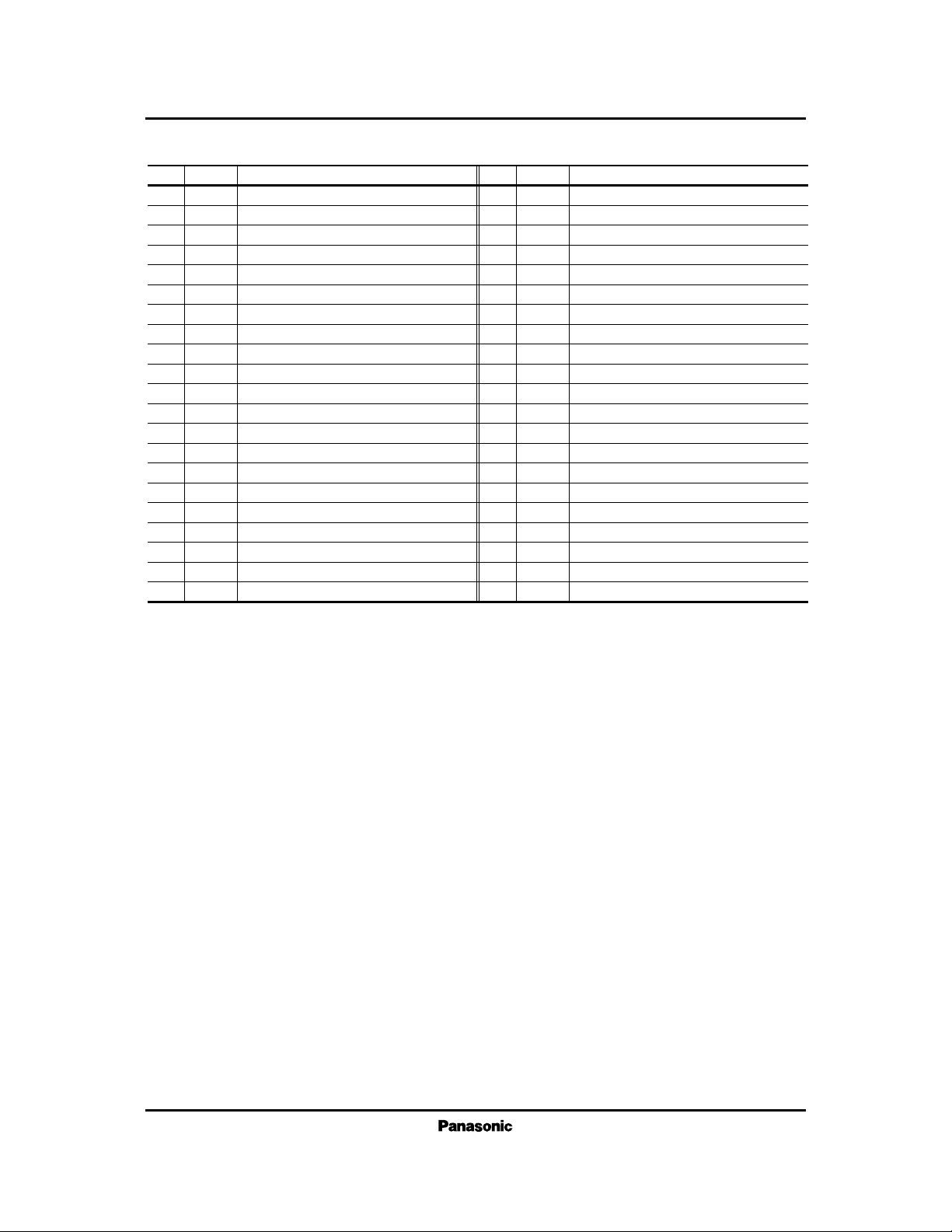
■ Block Diagram
V
V
Send
Vr1
L
Rec.2
–
+
Vr1
37
Vrl
40
Vrl
12
13
18
16
17
24
28
V
27
Vrl
11
38 39 19 14 15 41 42 36 34 29 6 5 35 1
Buff-
–
MA2
+
+
MA1
–
B
R
Log
Rec
Pre
–
+
V
B
TATT
AP
er
T
Log
V
B
+
–
+
–
Comp
AP
Buffer
V
CC1
Attenator
Control
–
Vr1
Rec.1
+
CC1
Power
Regulator
V
CC2
Power
Regulator
AGC
S.Amp
Power
Regulator
–
+
Vr2
GND
Matrix
33
Circuit
32
31
Matrix
Circuit
30
20
21
22
23
V
B
RATT
26
2543287910
2
ICs for Telephone
AN6426NK
■ Pin Descriptions
Pin No.
DescriptionSymbol
1
2
3
4
5
6
7
8
9
10
11
12
13
14
15
16
17
18
19
20
21
GND
AGC
SAO
SAI
Vr2
VPO
RO1
RO2
RBO
RPO
RPI
MAI1
MAO1
TL1
TLO
ND1
ND2
TAI
TAO
ATC
TAC
AC
RAC
RVR
RAO
RAI
RLO
RLI
V
CC
2
Mute (R)
HSu/SPu
Mute (S)
APC
Vr1
VB
VCC
MAO2
MAO2
TSI
MFI MF
S0
VL
Ground
Loudspeaker amp. time constant
Loudspeaker amp. output
Loudspeaker amp. input
Reference voltage (2)
Loudspeaker amp. power supply
Receiver output (1)
Receiver output (2)
Receiver buffer output
Receiver preamp. output
Receiver preamp. input
MIC amp. input (1)
MIC amp. output (1)
Transmitter LOG amp. input
Transmitter LOG amp. output
Noise detection time constant (1)
Noise detection time constant (2)
Transmitter att. input
Transmitter att. output
Att. timing control
Transmitter att. control
Pin No.
DescriptionSymbol
22
23
24
25
26
27
28
29
30
31
32
33
34
35
36
37
38
39
40
41
42
Att. control
Receiver att. control
To receiver rheostat
Receiver att. output
Receiver att. input
Receiver LOG amp. output
Receiver LOG amp. input
Supply voltage (2)
Receiver mute
HS/HF switching
Transmitter mute
Auto. PAD control
Reference voltage (1)
Reference voltage
Supply voltage (1)
MIC amp. input (2)
MIC amp. output (2)
Transmitter signal input
MF signal input
Transmitter output
Line voltage
3
ICs for Telephone
AN6426NK
V
L
I
L
P
D
T
opr
T
stg
Supply voltage
Supply current
Power dissipation (Ta = 60˚C)
Operating ambient temperature
Storage temperature
V
mA
mW
˚C
˚C
Parameter Symbol Rating Unit
■ Absolute Maximum Ratings (Ta=25˚C)
14.4
120
1700
–20 to + 60
–55 to +150
Note) The IC must be used under the condition PD>V
CC
× ICC.
Parameter Symbol Range
■ Recommended Operating Range (Ta=25˚C)
Operating supply voltage range
V
L
3V to 12V
Parameter Symbol Condition min typ max Unit
■ Electrical Characteristics (Ta=25˚C)
Power Supply
DC line voltage (1)
3.6V
L (1)
V
Voltage at Pin42 with IL=20mA
4.2 5.2
DC line voltage (2)
9.0V
L (2)
V
Voltage at Pin42 with IL=120mA
11.0 12.0
Int. supply voltage (1)
1.8V
CC (1)
V
Voltage at Pin36 with IL=20mA
2.3 2.8
Int. supply voltage (2)
6.0V
CC (2)
V
Voltage at Pin36 with IL=120mA
7.0 9.0
Int. regulated voltage (1)
0.95V
B (1)
V
Voltage at Pin35 with IL=20mA
1.10 1.35
Int. regulated voltage (2)
1.10V
B (2)
V
Voltage at Pin35 with IL=120mA
1.20 1.45
Trans. gain
26G
S
dB29 32
Rec. gain
36G
R
ni=–60dBm
input pin
output pin
11 7, 8
7, 8
dB39 42
Max. rec. level
4V
R
nO=4dBm
f
i
=1kHz,
ni=–25dBm
11
4242ni=–25dBm37
Att. rec. gain
–6.5G
ARR
dB–3.5 – 0.5
25 n
i
=–20dBm26
Max. trans. level
2.5V
S
dBm5.5 8.5
n
O
=2.5dBm37
7, 840
dBm
710
MF rec. gain
G
MR
9dB36
f
i
=1kHz,
nO=5dBm
7, 8
40
MF max. rec. level
V
MR
11 dBm58
Gain difference with
ni=
–60dBm as IL changes
between 30 and 80mA
7, 8
11
AP (R) characteristics
DG
R
–4 dB–8 –6
f
i
=1kHz,
ni=–25dBm
4240MF trans. gain G
MS
28 dB22 25
VPO=3V,
THD=5%
3
4
Loudspeaker amp. (1)
V
OSP (1)
dBm–10 –5
VPO=5V,
THD=5%
3
4
Loudspeaker amp. (2)
V
OSP (2)
dBm–4 1
VPO=7V,
THD=5%
3
4
Loudspeaker amp. (3)
V
OSP (3)
dBm04
f
i
=1kHz,
nO=1dBm
42
40
MF max. trans. level
V
MS
7 dBm14
Gain difference with
ni=–
25dBm as IL changes
between 30 and 80mA
42
37
AP (S) characteristics
DG
S
0dB–6 –4
V
24=V35
,
ni=–20dBm,
IL=60mA
25
26
Rheostat characteristics (1)
V
V
–22 dBm–28 –25
n
i
=–20dBm,
I20=14µA
T12–T11 Value
25
26
Att. trans. gain
G
ART
–28 dB–38 –33
HS
U
Receiver
HS
U
Transmitter
SPU Receiver
 Loading...