

Panasonic AN6263N, AN6262N Datasheet
ICs for Cassette, Cassette Deck
■ Overview
The AN6262N and the AN6263N are the pause detection integrated circuits which select the program on the
cassette tape. In the ordinal method, tape speed is different depending on the PLAY and FF/REW, and also nonsignal time between the programs is different. Therefore,
two time constant circuit has been applied in order to
detect each time. The AN6262N and the AN6263N are
proud of detecting the program by making the time corresponding to each non signal time logically in the one time
constant circuit. Furthermore, signal can be detected in
this time constant circuit and beginning of the program is
recognized when sound signal pulse increase more than
specified numbers.
■ Features
•
Built-in protection circuit to prevent mis-operation when
power switch is turned ON.
•
Time-constant circuit for detection of no-signal period
in PLAY and FF/REW.
•
No-signal period and output pulse width can be select-
ed by external capacitor.
•
Detection level of input signal can be selected by exter-
nal resistor.
•
As the ON/OFF input for mode setting and pause
detection, both TTL level and power source level can
be used.
•
Very few external components needed.
AN6262N, AN6263N
Pause Detection Circuits of Radio Cassette , Cassette Deck
9
8
7
6
5
4
3
2
0.3
+ 0.1
– 0.05
23.3±0.3
6.0±0.3
2.4±0.25
3.3±0.25
1.5±0.25
0.5±0.1
2.54
1.5±0.25
1.4±0.3
3.0±0.3
Unit : mm
30˚
1
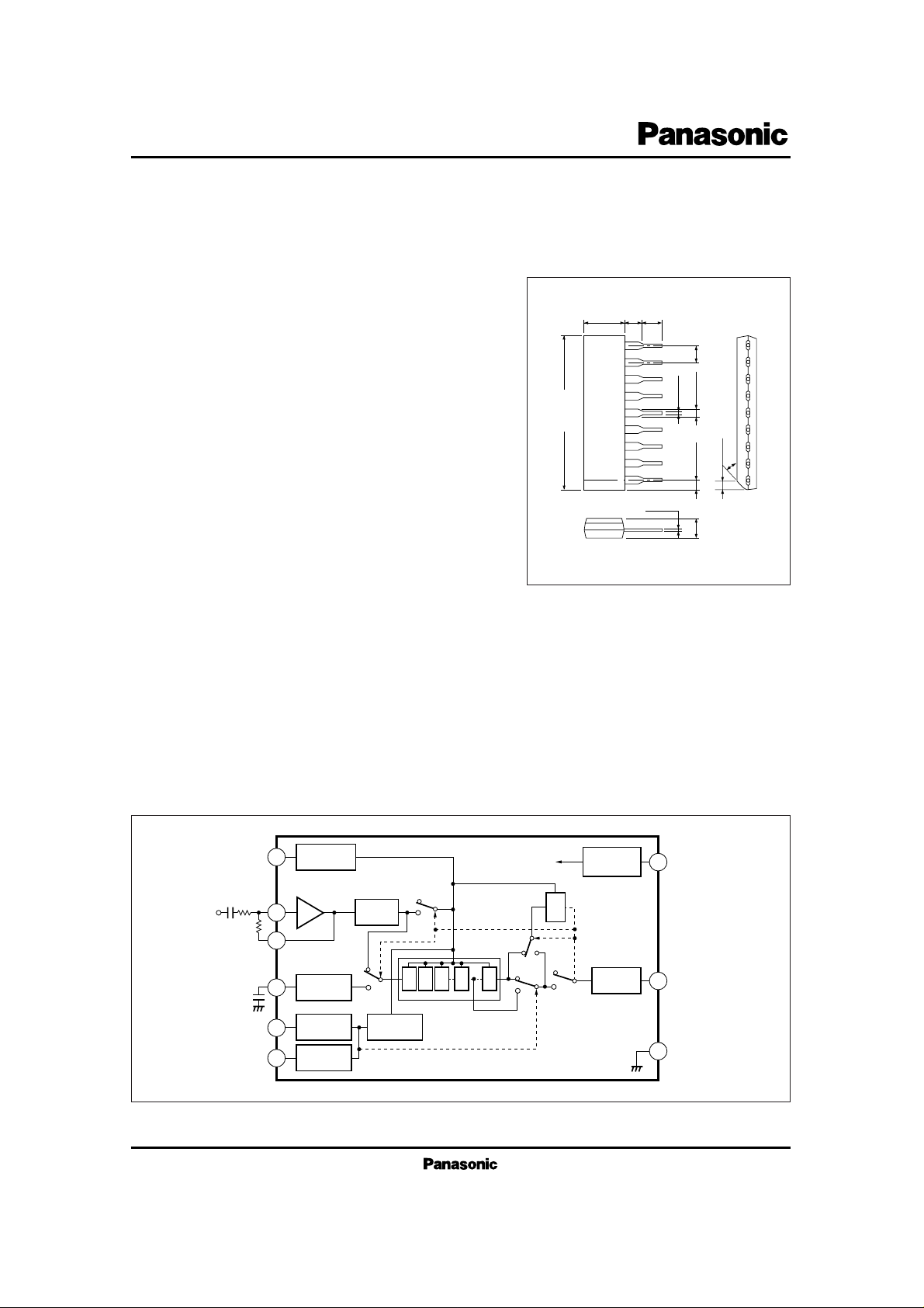
9-Lead SIP Package (SIP009-P-0000)
■ Block Diagram
Input
3
Circuit
a
SW
1–1
P
SW
Wave
Form
a
1–2
T
b
Differential
Circuit
FF1
b
FF2
FF3
Amp.
1
2
OSC
9
Input
7
Circuit
Input
8
Circuit
Reset
FF8
to each block
a
a
SW
FF12
b
SW
b
1–3
2
Voltage
Stabilizer
S
–
QT
FF
13
a
b
SW
Output
Circuit
1–4
V
CC
4
6
5
GND
ICs for Cassette, Cassette Deck
AN6262N, AN6263N
*
OFF
FF/REW
PLAY
OFF
Pin No.
Pin Name
1
2
3
4
5
6
7
8
9
Signal Input
Negative Feedback
Pause Detection ON/OFF Input
V
CC
GND
Output
Mode
*
Mode *
Reference Oscillation
■ Pin Descriptions
Pin 7
L
H
L
H
Pin 8
L
L
H
H
Mode
16
21
25
336
475
–25 ~ + 75
–55 ~ + 125
V
CC
Supply Voltage
Supply Current
Power Dissipation
Operating Ambient Temperature
Storage Temperature
V
mA
mA
mW
mW
˚C
˚C
Parameter Unit
AN6262N
AN6263N
AN6262N
AN6263N
I
CC
P
D
T
opr
T
stg
Symbol Rating
Parameter Symbol Condition min. typ. max. Unit
■ Electrical Characteristics (VCC=12V, Ta=25˚C)
Supply Current (Output OFF)
Oscillation Frequency
Signal Detection Level
Pause Detection ON/OFF Level
Pause Detection OFF Outcoming Current
Mode Switching
Level
Mode Switching Circuit
Outgoing Current
V
3=V7=V8
=2V,
V
9
=1V
V
1
=0V, V3=V7=V8=0V
f
1
=10kHz, V3=V7=2V, V8=0V
I
3
= –100µA, V7=V8=2V, V9=1V
V3=
0V, VCC=
18V, V7=
V8=
2V, V9=
1V
V3=V8=2V, I7= –100µA, V9=1V
V
3=V7
=2V, I8= –100µA, V9=1V
V3=
V8=
2V, VCC=
18V, V7=
0V, V9=
1V
V
3
=
V7=
2V, VCC=
18V, V8=
0V, V9=
1V
I
4 (OFF)
f
OSC
V
1
V
3–5
I
3
V
7–5
V
8–5
I
7
I
8
Pin7
Pin8
Pin7
Pin8
AN6262N
AN6263N
11.5
12.5
0.9
1.6
1.1
– 0.6
1.0
1.0
–1.2
–1.2
1.2
20
23
1.47
2.6
1.6
– 0.3
1.5
1.5
– 0.6
– 0.6
mA
mA
kHz
mVrms
V
mA
V
V
mA
mA
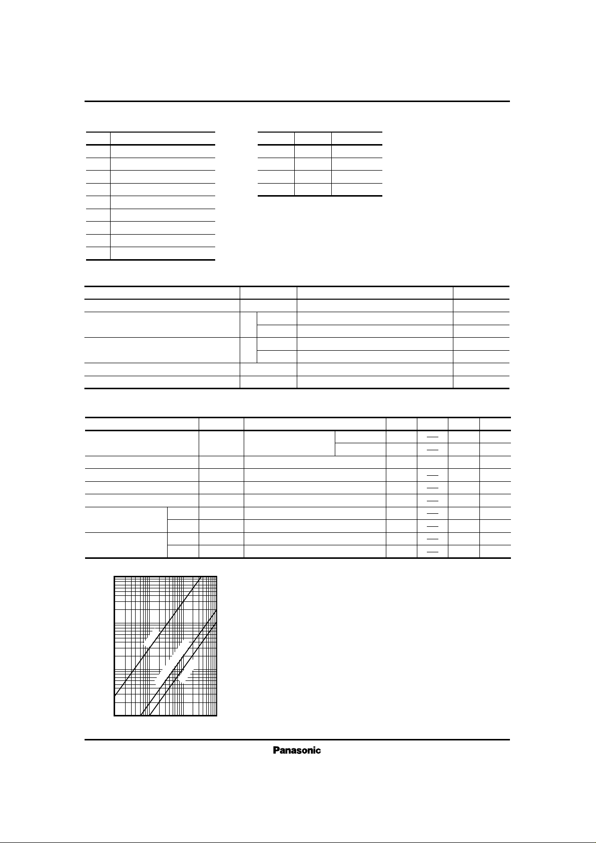
t – C
0.01
0.001
0.3
1
3
10
0.003
Oscillation Capacitance C (µF)
Time of non-signal period t (s)
0.1
0.03
0.01 0.03 0.1 0.3 1
FF/REW
PLAY
Output Pulse Width
 Loading...