

Panasonic AN6215S Datasheet
ICs for Telephone
AN6215S
AGC IC for telephone speech network
■ Overview
The AN6215S is an AGC IC for telephone speech
network, and it incorporates an microphone input detection circuit and a receiver gain control circuit. It is especially best suited for cordless telephone thanks to a good
speech tone quality obtained by reducing howling and echo
sound.
■ Features
• Operation with wide power supply voltage range from
2.1 V to 6.0 V
• Enlargement of dynamic range by incorporating a
able V
circuit that varies according to the supply
REF
voltage
• Possible to adjust the received voice attenuation amount
with an external resistor
• Possible to adjust the AGC operating point with an ex-
ternal resistor
• Possible to design with fewer external components
vari-
0.4 ± 0.25
1
2
0.6 ± 0.3
3
1.27
4
0.3
0.1 ± 0.1
8
7
6
5
4.2 ± 0.3
6.5 ± 0.3
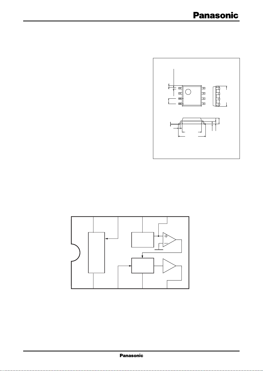
SOP008-P-0225A
Unit: mm
0.15
0.65
5.0 ± 0.3
1.5 ± 0.2
■ Block Diagram
8
V
1
CC
V
REF
GND
7
6
5
Det.
CC
2
3
Buff
4
1
AN6215S ICs for Telephone
■ Pin Descriptions
Pin No. Symbol Description
1 GND Ground pin
2 ∆GAIN Variable gain adjustment pin
3 RX IN Receiver signal input pin
4 RX OUT Receiver signal output pin
5 TX DET Transmitter signal detection pin
6 TX IN Transmitter signal input pin
7VCV
8VCCSupply voltage pin
■ Absolute Maximum Ratings
Parameter Symbol Rating Unit
Supply voltage V
Supply current I
Power dissipation P
Operating ambient temperature
Storage temperature
Note)*: Except for the operating ambient temperature and storage temperature, all ratings are for Ta = 25°C.
*
control pin
REF
*
CC
CC
D
T
opr
T
stg
6.5 V
3.0 mA
19.5 mW
−20 to +75 °C
−55 to +125 °C
■ Recommended Operating Range
Parameter Symbol Range Unit
Supply voltage V
CC
2.1 to 6.0 V
■ Electrical Characteristics at Ta = 25°C
Parameter Symbol Conditions Min Typ Max Unit
1
Operating current
Receiver amp. voltage gain
Receiver amp. output D range
Receiver amp. ∆Gain Receiver amp. gain variation between −10 −8 −6dB
variable gain width
High-level V
High-level V
Low-level V
Note) 1. VCC = 5.0 V, f = 1 kHz unless otherwise specified.
2.*1: Pin 7 DC voltage sets to VCH = 5.0 V
2: ERO-25CKF6802 produced by Matsushita Electronic Components Co. is used for RX in = −30 dBm.
*
*
1
*
*
2
*1, *
control sink current I
REF
control voltage V
REF
control voltage V
REF
(Refer to " ■Application circuit example".)
I
CC
G
RX
1
V
ORX
CH
CH
CL
Operating time at no signal input 1.4 2.0 mA
RX in = −20 dBm 1.5 3.5 5.5 dB
Output voltage at THD = 5% 0 2 dBm
TX in = −50 dBm and TX in = −30 dBm
VCH = 3 V 25 50 µA
Pin 7 voltage range in a base-set mode 1.5 V
CC
V
Pin 7 voltage range in a hand-set mode 0 0.5 V
2
 Loading...