Panasonic AN6175K Datasheet
1
ICs for Telephone
■ Overview
The AN6175K is a speech network IC incorporating a
hands-free function. It provides for a high-quality handsfree telephone or handset telephone. The hands-free
telephone function(HF)includes :
• MIC amplifier capable of mute and gain control
• Background noise monitoring
• Voice switching attenuation control
• Symmetrical transmitter/receiver attenuators
• Dynamic loudspeaker amplifier
The handset telephone function(HF)includes:
• Automatic pad capable of detecting transmission
distance
• MIC amplifier
• Receiver preamplifier
• Dynamic loudspeaker amplifier
■ Features
•
Provides all the functions required of a hands-free or
handset telephone.
•
Can operate on line voltage (requiring no external
power supply).
•
Consumes minimal current.
•
Provides for an external filter ensuring a wide range of
howling suppression.
•
Mute mode for hands-free operation
•
Background noise monitoring to improve transmission
quality
•
100 mW loudspeaker output (at IL=100mA)
•
Built-in power supply and low-voltage regulator
•
DIP package with 42-pins or QFH package with 44-pins
AN6175K
Hands-free Speech Network IC
3 ∼ 15
°
Unit : mm
15.3±0.25
0.3
+0.1
−0.05
AN6175K
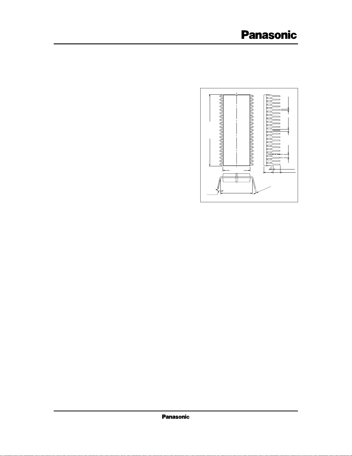
SDIP package with 42 pins (SDIP042-P-0600A)
36.8±0.3
0.9±0.25
13.7±0.3
0.5±0.1
1.778
4.76±0.25 3.3±0.25
0.96±0.25
42
41
40
39
38
37
36
35
34
33
32
31
30
29
28
27
26
25
24
23
22
1
2
3
4
5
6
7
8
9
10
11
12
13
14
15
16
17
18
19
20
21
2
ICs for Telephone
AN6175K
42 41 40 39 38 37 36 35 34 33 32 31
33
30 29 28 27 26 25 24 23 22
1 2 3 5 6 7 8 9 10 11 12 13 14 15 16 17 18 19 20 21
TAPC
Vr CONT
+
−
INT
BGR
V
CC
+
−
RAPC
ATT
CONT
TND
+
−
+
−
+
−
DIAPCRAOTAOATCRVRCONT
REC−
RLO2RLO1TLO2TLO1RLI2RLI1TLI2TLI1TVRTND
LOG5
(HS)
MAO
(HS)
MAI
(HF)
MAI
(HF)
MAO
SOUT V
CC
1 BGR TRE TRB V
CC
2 HFI MFI ST Vr HS/HF HS,HF
/MF
RPI RPO VSP SPI FB SPO1 SPO2 GND DO
Vr Vr
SP Pre
SP
Vr
RATT
COUNT1COUNT2
LOG1
Vr
VrVr
LOG2 LOG4 LOG3
TATT
41
4040
41
+
IL
VL
V
CC
1
4
+
−
+
−
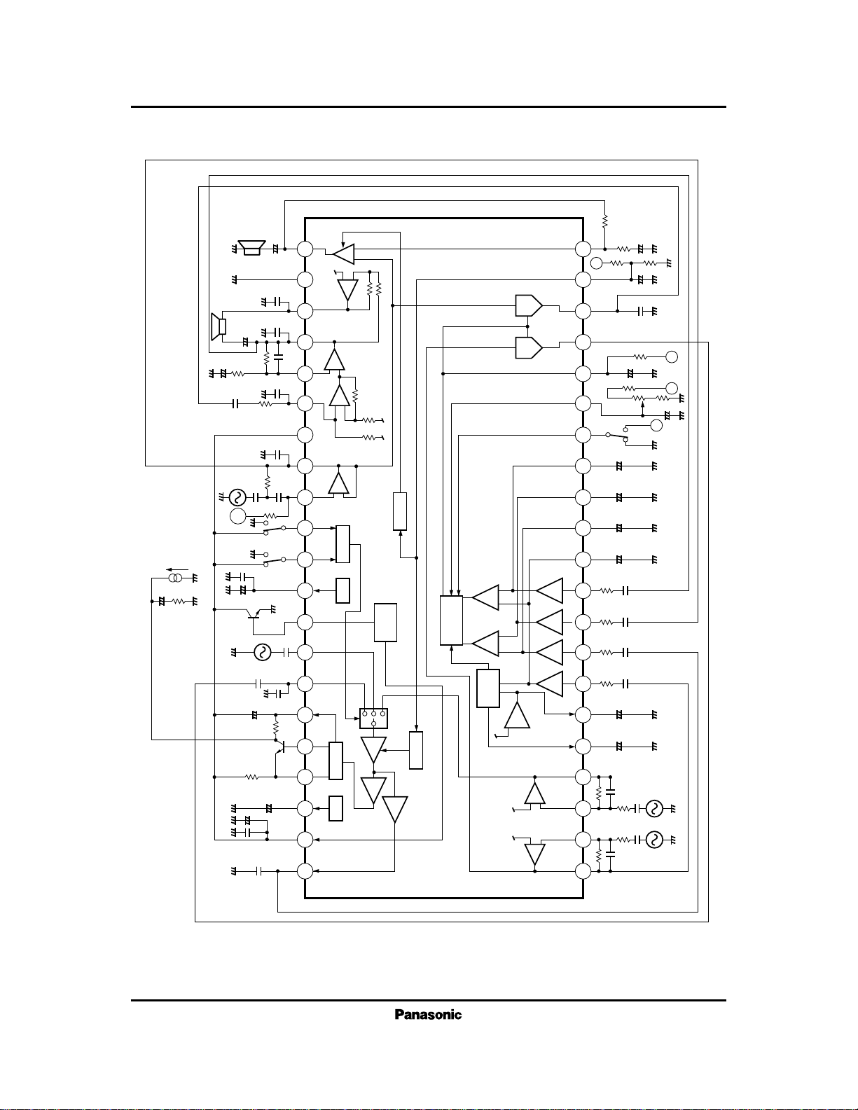
■ Block Diagram
3
ICs for Telephone
AN6175K
V
CC2
I
L
P
D
T
opr
T
stg
Supply voltage
Supply current
Power dissipation
Note)
Operating ambient temperature
Storage temperature
V
mA
mW
°C
°C
Parameter Symbol Rating Unit
■ Absolute Maximum Ratings (Ta=25°C)
12.0
120
1016
–20 to + 75
–55 to + 150
Note) In an open condition with Ta=25°C
■ Pin Descriptions
Pin No.
DescriptionSymbol Symbol
1
2
3
4
5
6
7
8
9
10
11
12
13
14
15
16
17
18
19
20
21
22
23
24
25
26
27
28
29
30
31
32
33
34
35
36
37
38
39
40
41
42
Pin No.
Description
MAO
(HF)
MAI
(HF)
MAI
(HS)
MAO
(HS)
MIC amp. output (hands-free mode)
MIC amp. input (hands-free mode)
MIC amp. input (handset mode)
MIC amp. output (handset mode)
Hands-free mode transmission noise detection
Noise detection reference
LOG amp. (1) input (from MIC amp. output)
LOG amp. (1) output
LOG amp. (2) output
LOG amp. (3) output
LOG amp. (4) output
Receiver switching (hands-free mode)
Receiver att. gain control
Receiver att. switching control
Transmitter att. output (hands-free mode)
Receiver att. output (hands-free mode)
Receiver amp. input (–)
TND
TVR
TLI1
TLI2
RLI1
RLI2
TLO1
TLO2
RLO1
RLO2
DO
GND
SPO2
SPO1
FB
SPI
VSP
RPO
RPI
HS/HF
Vr
ST
MFI
HFI
V
CC2
TRB
TRE
BGR
V
CC1
SOUT
REC–
CONT
RVR
ATC
TAO
RAO
APC
DI
Receiver amp. output
Ground
Loudspeaker amp. (2) output
Loudspeaker amp. (1) output
Loudspeaker amp. input (–)
Loudspeaker amp. input (+)
Loudspeaker amp. power input
Receiver preamp. output
Receiver preamp. input
Mode switching (handset or hands-free/MF)
Mode switching (handset/hands-free)
Reference for handset or hands-free mode
To the base of the power supply transistor
MF input
From transmitter att. output (hands-free mode)
Transmission amp. AC impedance setting
To the base of the transmission transistor
To the emitter of the transmission transistor
Band-gap ref. voltage output
Hands-free control output
HS,
HF/MF
LOG amp. (2) input
(from hands-free control output)
LOG amp. (4) input
(from receiver preamp. output)
LOG amp. (3) input
(from loudspeaker amp. output)
Auto. PAD current control
(handset mode, MF)
Power output to the handset and hands-free
circuits
4
ICs for Telephone
AN6175K
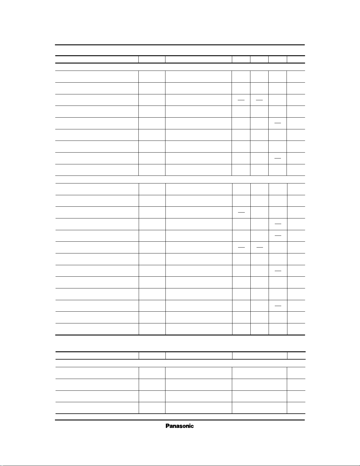
Parameter Symbol Condition min typ max
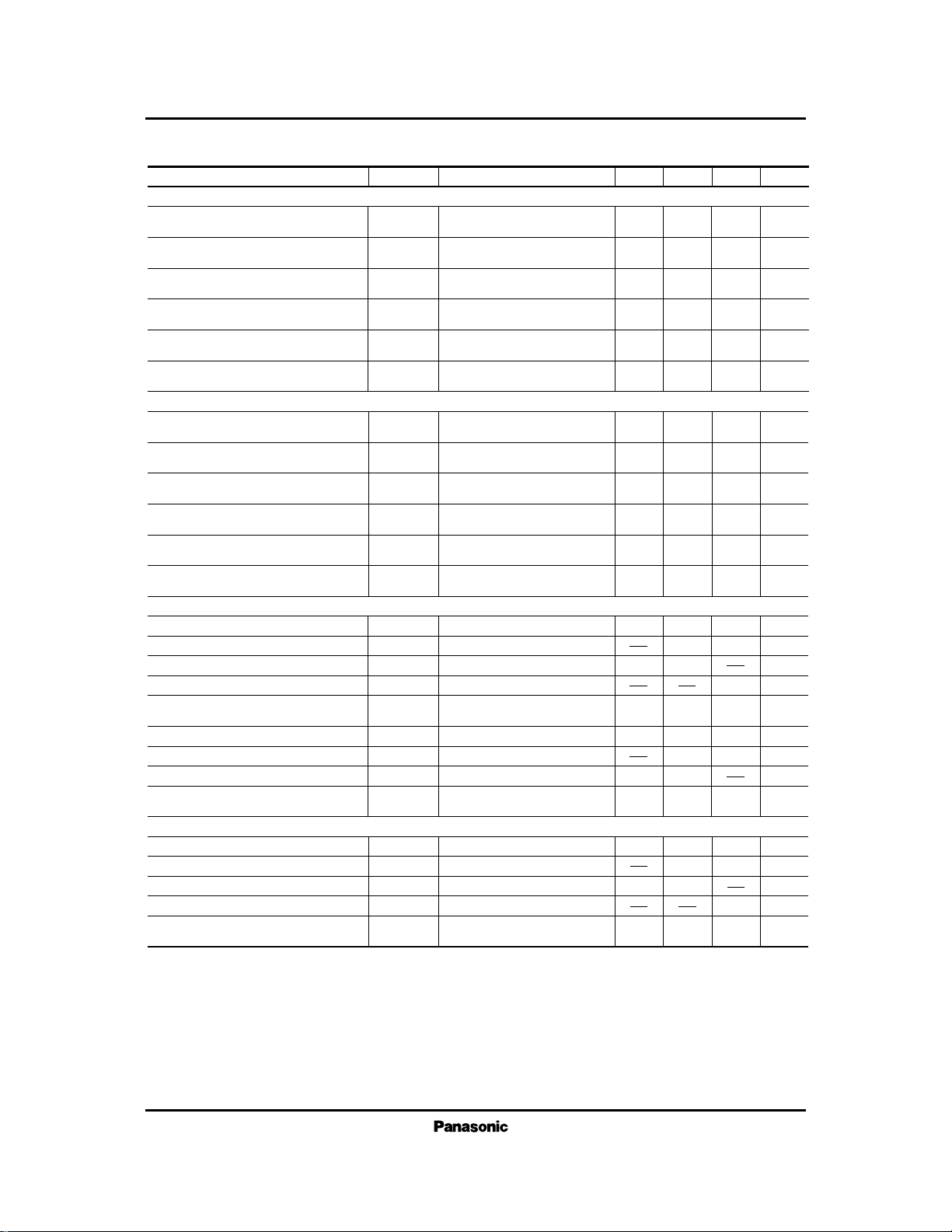
■ Electrical Characteristics (Ta=25±2°C)
HS mode line voltage (1)
HS mode line voltage (2)
HS mode V
CC
2 voltage (1)
HS mode V
CC
2 voltage (2)
HS mode V
CC
1 voltage (1)
HS mode V
CC
1 voltage (2)
V
LS1
V
LS2
V
CS21
V
CS22
V
CS11
V
CS12
V4.0
SW1,2 : a
I
L
= 20mA, VL voltage
SW1/2 : a/a
I
L
= 120mA, VL voltage
SW1/2 =a/a,
I
L
= 20mA, DC voltage at pin37
SW1/2 =a/a,
IL=
120mA, DC voltage at pin
37
SW1/2 =a/a,
I
L
= 20mA, DC voltage at pin41
SW1/2 =a/a,
IL=
120mA, DC voltage at pin
41
4.4
HS power supply
HF power supply
3.6
V10.5 11.59.5
V3.7 4.13.3
V9.3 10.38.3
V2.0 2.41.6
V4.8 5.24.4
HF mode line voltage (1)
HF mode line voltage (2)
HF mode V
CC
2 voltage (1)
HF mode V
CC
2 voltage (2)
HF mode V
CC
1 voltage (1)
HF mode V
CC
1 voltage (2)
V
LF1
V
LF2
V
CF21
V
CF22
V
CF11
V
CF12
V4.0
SW1/2=a/b,
I
L
= 20mA, VL voltage
SW1/2=a/b,
I
L
= 120mA, VL voltage
SW1/2=a/b,
I
L
= 20mA, DC voltage at pin37
SW1/2=a/b,
IL=
120mA, DC voltage at pin
37
SW1/2=a/b,
I
L
= 20mA, DC voltage at pin41
SW1/2=a/b,
IL=
120mA, DC voltage at pin
41
4.43.6
V10.5 11.59.5
V3.7 4.13.3
V9.3 10.38.3
V2.0 2.41.6
V4.8 5.24.4
Unit
Trans. amp. gain
MF trans. amp. auto. PAD
GHS
APMF
dB29
Vin1= –30dBm
Gain Difference with
Vin2
= –
30dBm, IL=
20 to 120mA
31
HS transmitter
27
Trans. amp. distortion
THS %0.3
Vin1= –30dBm
2.0
Trans. amp. max output
VHS dBm2.5
THS= 5%
– 0.5
Trans. amp. noise
NHS dBm
Rg= 2kΩ with a CCITT filter
–65
MF trans. amp. gain
GMF dB29
Vin2= –30dBm
3127
MF trans. amp. distortion
TMF %0.3
Vin2= –30dBm
2.0
MF trans. amp. max output
VMF dBm3.0
TMF= 5%
0
dB6 84
Trans. level auto. PAD
APS
Gain Difference with
Vin1
= –
30dBm, IL=
20 to 120mA
dB6 84
HS receiver
Rec. amp. gain
GHR dB19
Vin3= –35dBm
2117
Rec. amp. distortion
THR %1.5
Vin3= –35dBm
5
Rec. amp. max output
VHR dBm–7
THR= 5%
–10
Rec. amp. noise
NHR dBm
Rg=2kΩ with a CCITT filter
–75
Rec. amp. auto. PAD
APR
Gain Difference with
Vin3
= –
35dBm, IL=
20 to 120mA
dB6 84
Note: Unless otherwise specified, IL=20 mA and fin=1 kHz.
5
ICs for Telephone
AN6175K
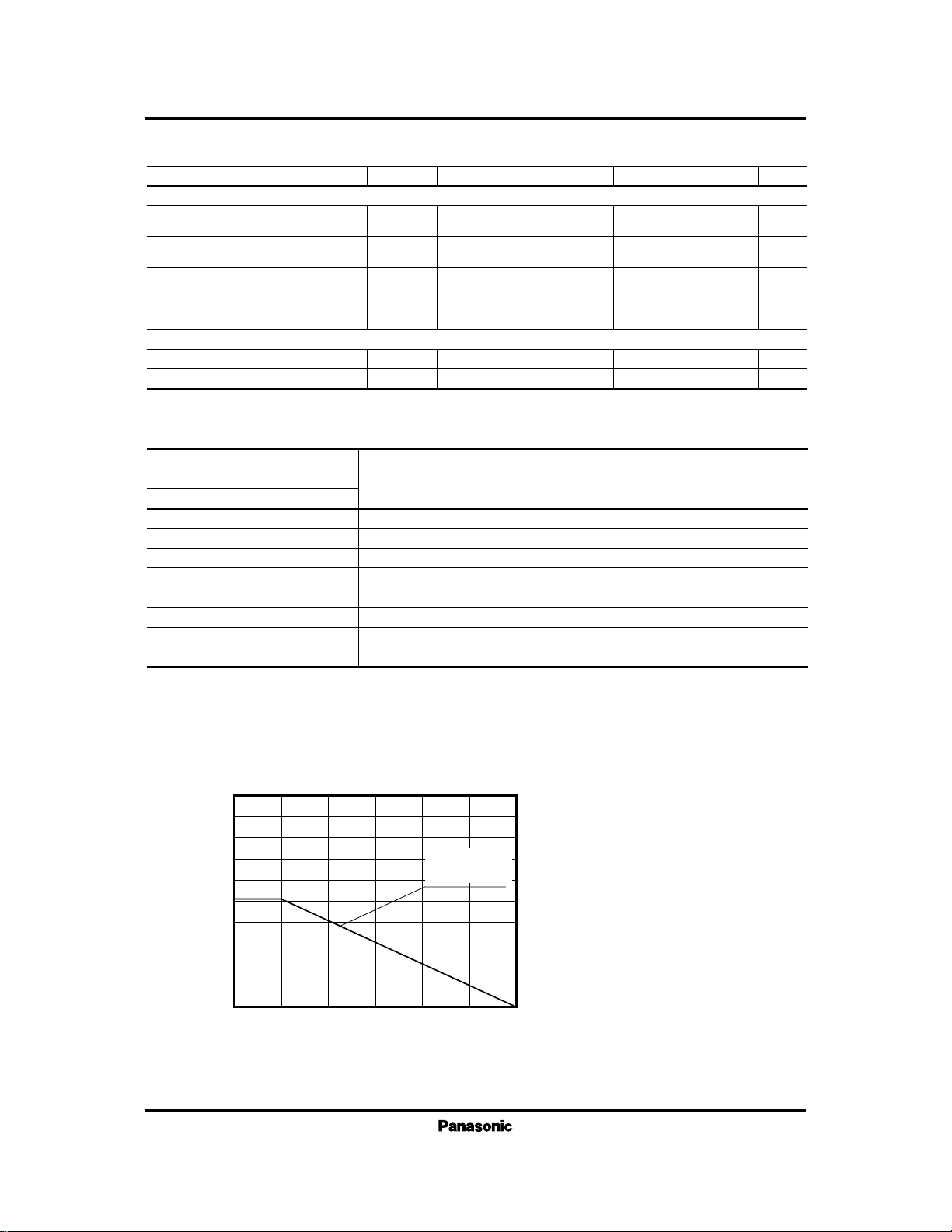
Parameter Symbol Condition min typ max
■ Electrical Characteristics (cont.) (Ta=25±2°C)
Unit
Trans. gain (1)
G
FS1
Vin4= –65dBm
I
L
=20mA
HF transmitter
dB60 6357
Trans. gain (2)
G
FS2
Vin4= –65dBm
I
L
=120mA
dB66 6963
Trans. noise
N
FS
Rg=2kΩ,
I
L
=20mA with a CCITT filter
dBm–58
Trans. att. gain (1)
G
TA MAX1
Vin4= –60dBm
I
L
=20mA
dB31 3428
Trans. att. gain range (1)
Trans. att. idling gain (1)
G
TA MIN1
Vin4= –60dBm
I
L
=20mA
dB4845
G
TA IDL1
Vin4= –60dBm
I
L
=20mA
dB4 71
Trans. att. gain (2)
G
TA MAX2
Vin4= –60dBm
I
L
=20mA
dB36 3933
Trans. att. gain range (2)
Trans. att. idling gain (2)
G
TA MIN2
Vin4= –60dBm
I
L
=20mA
dB5047
G
TA IDL2
Vin4= –60dBm
I
L
=20mA
dB6 93
Rec.gain (1)
G
FR1
Vin3= –50dBm
I
L
=20mA
HF receiver
dB37 4034
Rec. gain (2)
G
FR2
Vin3= –50dBm
I
L
=120mA
dB43 4640
Rec. distortion
TSP
Vin3= –50dBm
I
L
=20mA
%1.5 5.0
Rec. max output (1)
V
SP1
TSP=5%, IL=20mA
dBm–7–10
Rec. max output (2)
Rec. noise
V
SP2
TSP=5%, IL=120mA
dBm74
N
FR
Rg=2kΩ,
I
L
=20mA with a CCITT filter
dBm–60
Rec. att. gain (1)
G
RA MAX1
Vin3= – 40dBm
I
L
=20mA
dB12 159
Rec. att. gain range (1)
Rec. att. idling gain (1)
Rec. att. gain (2)
Rec. att. gain range (2)
Rec. att. idling gain (2)
Rec. att. volume characteristics
G
RA MIN1
Vin3= – 40dBm
I
L
=20mA
dB5249
G
RA IDL1
Vin3= – 40dBm
I
L
=20mA
dB–12 –9–15
G
RA MAX2
Vin3= – 40dBm
I
L
=120mA
dB17 2014
G
RA MIN2
Vin3= – 40dBm
I
L
=120mA
dB5653
G
RA IDL2
Vin3= – 40dBm
I
L
=120mA
dB–10 –7–13
G
RA VRM
Vin3= – 40dBm
I
L
=20mA
dB–2 0–4
1.0
2.0
1.17
610
HS mode internal reference voltage (1)
V
rs
Pin31 high, Pin32 high,
I
L
=20mA
HS power supply
V
HS mode internal reference voltage (2)
V
SPS
Pin31 high, Pin32 high,
I
L
=20mA
V
HS mode internal reference voltage (3)
V
BGS
Pin31 high, Pin32 high,
I
L
=20mA
Pin31 high, Pin32 high,
I
L
=20mA
V
HS mode AC impedance
Z
ACS
Ω
Parameter Symbol Condition Design value
■ Electrical Characteristics (Design Values for Reference) (Ta=25±2°C)
Unit
6
ICs for Telephone
AN6175K
31
HF, HS/MF
0
0
0
0
1
1
1
1
32
HS/MF
0
0
1
1
0
0
1
1
Description
Pin No.
Where 0 means connection to GND, and 1 means connection to Pin41(V
CC
1).
15
REC– CONT
0
1
0
1
0
1
0
1
Transmit MF in the hands-free mode. Trans./rec. att. can be changed according to input level.
Transmit MF in the hands-free mode. Trans./rec. att. is available only in the receiver mode.
Transmit MF in the handset mode.
Transmit MF in the handset mode.
Speech in the hands-free mode
Speech in the hands-free mode. Trans./rec. att. is available only in the receiver mode.
Speech in the handset mode
Speech in the handset mode
■ Mode Control
0
200
400
600
1,000
1,200
1,400
1,600
1,800
(mW)
0 25 50 10075 125 150
Ambient Temperature (Ta)
Power Dissipation (P
D
)
(°C)
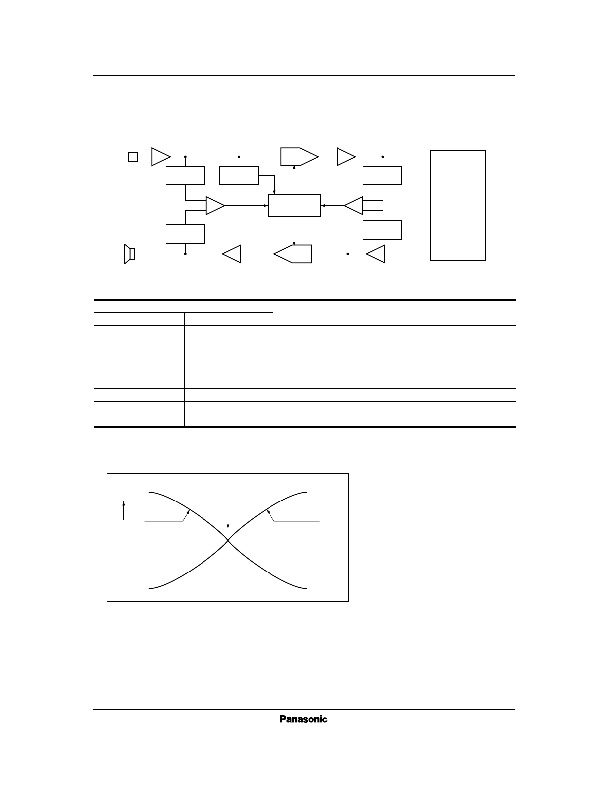
Open condition
Rthj— a=123°C/W
P
D
=1016mW(25°C)
P
D
Ta
800
1016
■ ES-42D Package Power Dissipation
Parameter Symbol Condition Design value
■ Electrical Characteristics (Design Values for Reference) (cont.) (Ta=25±2°C)
HF power supply
Control voltage
1.0
2.0
1.17
610
– 0.3 to + 0.5
1.0 to 5.0
Unit
HF mode internal reference voltage (1)
V
rF
Pin31 high, Pin32 low,
I
L
=20mA
V
HF mode internal reference voltage (2)
V
SPF
Pin31 high, Pin32 low,
I
L
=20mA
V
HF mode internal reference voltage (3)
V
BGF
Pin31 high, Pin32 low,
I
L
=20mA
Pin31 high, Pin32 low,
I
L
=20mA
V
HF mode AC impedance
Z
ACF
Ω
Low level
V
C
(L) V
High level
Note) These values are for reference only (not guaranteed values).
V
C
(H) V
7
ICs for Telephone
AN6175K
TLOG2
Attenuator Control
Trans. Level
Monitor
Rec. Level
Monitor
Noise Level
Monitor
MIC Level
Monitor
SP Level
Monitor
RLOG1
TLOG1
RLOG1
SP
MIC
Rec. Attenuator
Trans. Attenuator
Line Interface
C1 C2
■ Operation in the Hand-free Mode
• Block Diagram
C1
TX
TX
RX
RX
TX
TX
RX
—
C2
TX
RX
TX
RX
TX
RX
TX
—
Input signal
Operation mode
C1 : Output comparison between TLOG1 and RLOG1.
C2 : Output comparison between TLOG2 and RLOG2.
Trans. noise
TX
TX
TX
—
noise
noise
noise
—
REC– CONT
0
0
0
0
0
0
0
1
Transmitter mode
High-speed switching idle mode
High-speed switching idle mode
Receiver mode
Low-speed switching idle mode
Low-speed switching idle mode
Low-speed switching idle mode
Receiver mode
■ Attenuator Control
Receiver Gain Transmitter Gain
Idle Mode
■ Trans./Rec. Switching Characteristics
Gain
 Loading...