

Panasonic AN6167SB, AN6167S Datasheet
■ Overview
The AN6167S and AN6167SB are speech network ICs for
the handset of a cordless telephone. They incorporate compander, MIC, and receiver amplifiers. With a minimal number of
external components, they can perform all the functions of the
handset of a cordless telephone featuring low radio-transmission noise.
■ Features
•
The compressor/expander circuit incorporates preamplifiers
to make level and frequency adjustments easier.
•
The standby circuit provides for a low-power consumption
cordless telephone.
•
The expander has a 6-dB amplifier to allow received-signal
amplificaition.
•
SOP package with 1.27mm pitch pins, and USO package
with 0.8mm pitch pins.
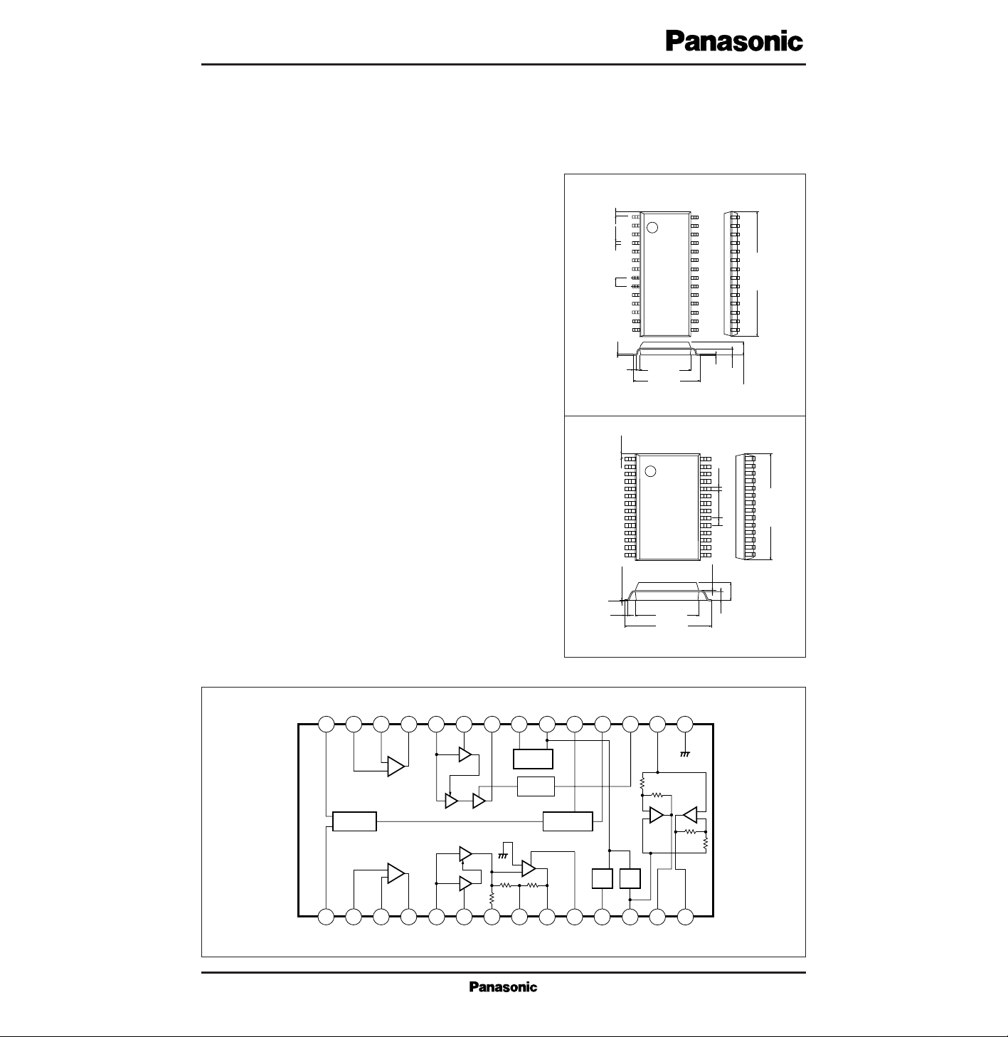
AN6167S, AN6167SB
Cordless Telephone Speech Network IC
Unit : mm
AN6167S
SOP package with 28 pins (SOP028-P-0375A)
1
2
3
4
5
6
7
10
11
12
13
14
8
9
28
27
26
25
24
23
22
21
20
19
18
17
16
15
0.45
0.4±0.25
1.27
17.81±0.3
0.1±0.1
2.0±0.2
0.925
0.15
0.3
7.2±0.3
9.4±0.3
■ Block Diagram
Unit : mm
AN6167SB
SSOP package with 28 pins (SSOP028-P-0375)
1
14
28
15
(0.45)
11.6±0.3
0.3±0.1
0.8
2.0±0.2
0.1±0.1
0.9
0.15
0.3
7.2±0.3
9.3±0.3
VCCEPIE
28 27 26 25 24 23 22 21 20 19 18 17 16 15
1
GNDC
POWER
2
C
PICPNCPOCCCACDETCINCORCOUT
EPOE
PN
–
+
+
–
3 4 5 6 7 8
CCAEDETEOUTEREFVREF
DET
E
CCA
CCA
C
DET
STC STBV DG
VR
E
D6dB
STBY
+
–
9 10 11 12 13 14
VR
C
C
C
REF
PC
R
IN
–
+
REC
VR
R
R
REFRO –2RO –1
GNDG
REC
+
–
V
CC
V
in
V
out
P
D
T
opr
T
stg
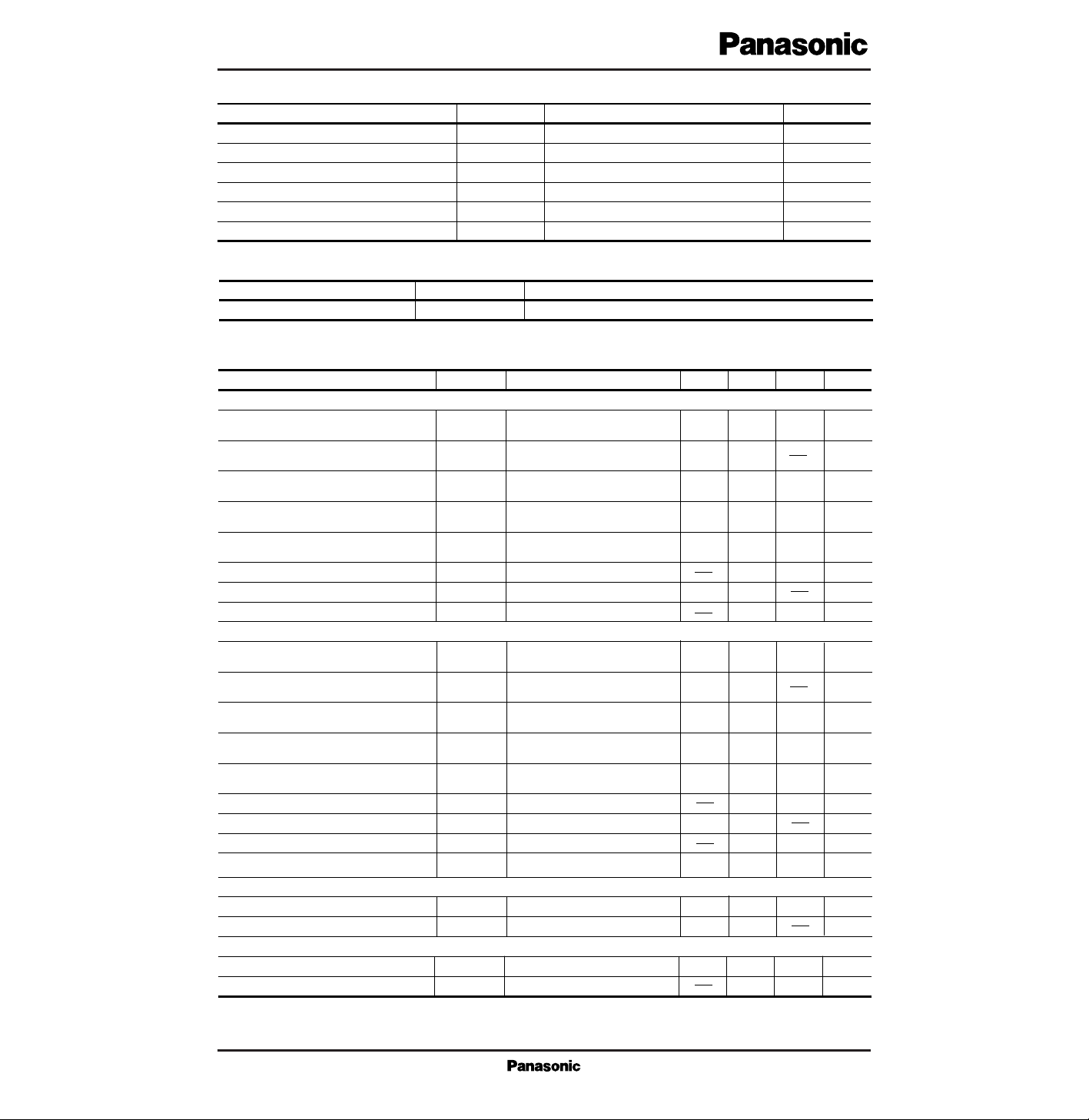
Supply voltage
Input supply voltage
Output supply voltage
Power dissipation (Ta = 75˚C)
Operating ambient temperature
Storage temperature
V
V
V
mW
˚C
˚C
Parameter Symbol Rating Unit
■ Absolute Maximum Ratings (Ta=25˚C)
7.5
– 0.3 to V
CC
+ 0.3
– 0.3 to V
CC
+ 0.3
280
–20 to + 75
–55 to +150
Parameter Symbol Range
■ Recommended Operating Range (Ta=25˚C)
Operating supply voltage range
V
CC
2 to 5V
Parameter Symbol Condition min typ max Unit
■ Electrical Characteristics (Ta=25˚C)
Compressor
Expander
Preamplifier voltage gain
G
PC
22 dB
RA/RB=51kΩ/5.1kΩ,
V
in
=–40dBV
20 21
Preamplifier output voltage
V
PC
dBV
RA/RB=51kΩ/5.1kΩ,
THD=5%, R
L
=1kΩ
–10 –7
Maximum output voltage
–10V
OCM
dBV
Output noise voltage V
NOC
dBV
Receiver amplifier
Distortion
THD
C
Vin=–20dBV
THD=5%, RL=1kΩ
Rg=2kΩ
with a CCITT filter
0.5
–7
1 %
–56–64
Reference output
V
ORC
–9 dBV
V
IRC
=–20dBV
(Ref. output)
–13 –11
∆ Gain (1)
∆C
1
–9 dB
Vin=V
IRC
–20dB,
∆C
1=VORC–VOC1
–11 –10
Preamplifier voltage gain
G
PE
22 dB
RA/RB=51kΩ/5.1kΩ,
V
in
=–40dBV
20 21
Preamplifier output voltage
G
PE
dBV
RA/RB=51kΩ/5.1kΩ,
THD=5%, R
L
=1kΩ
–10 –7
Reference output
V
ORE
–26 dBV
V
IRE
=–20dBV
(Ref. output)
–32 –29
∆ Gain (1)
∆E
1
–19 dB
Vin=V
IRC
–10dB,
∆E
1=VORE–VOE1
–21 –20
∆ Gain (2)
∆E
2
–38.5 dB
Vin=V
IRC
–20dB,
∆E
2=VORE–VOE2
–41.5 –40
∆ Gain (2)
∆C
2
–19 dB
Vin=V
IRC
–40dB,
∆C
2=VORC–VOC2
–22 –20
Receiver amp. gain
∆G
E
Pin17 ON [GND]
4 6 8 dB
Maximum output voltage
–10V
OFM
dBV
Output noise voltage V
NOE
dBV
Distortion
THD
E
Vin=–20dBV
THD=5%, RL=1kΩ
Rg=2kΩ
with a CCITT filter
0.5
–7
1 %
–90–95
Power supply
Receiver voltage characteristics
G
VR
Vin=–30dB, RL=1kΩ
18 20 22 dB
Current consumption
I
CC
VCC=3V, no signal
3 5 8 mA
Receiver voltage characteristics
I
SC
Standby pin (H)
1 10 µA
Maximum output voltage
V
OEM
THD=5%, RL=1kΩ
2 5 dBV
 Loading...