

查询AN5829供应商
ICs for TV
AN5829S
Sound multiplex decoder IC for the U.S. televisions
■ Overview
The AN5829S is a multiplex sound demodulation IC
dedicated to the U.S. television and incorporates a bidirectional I
2
C interface (adjustment, mode SW), an AGC
circuit and external stereo input switches (2 systems).
■ Features
• Stereo demodulation, SAP demodulation, dbx noise re-
duction, AGC, external stereo input SW and I
interface are integrated in a single chip
• Bi-directional I
2
C bus makes it possible to monitor
MPX input level, separation adjustment (3 places), mode
changeover and receiving status.
• Eliminated external parts (multi-sound block: 21 pieces
→ 14 pieces
• Lower power dissipation (V
= 5 V, I
CC
TOT
2
C bus
= 18 mA)
■ Applications
• Televisions and VCRs for the North American market
0.3
0.4±0.25 0.451.27
10
11
12
0.1±0.1
1
2
3
4
5
6
7
8
9
24
23
22
21
20
19
18
17
16
15
14
13
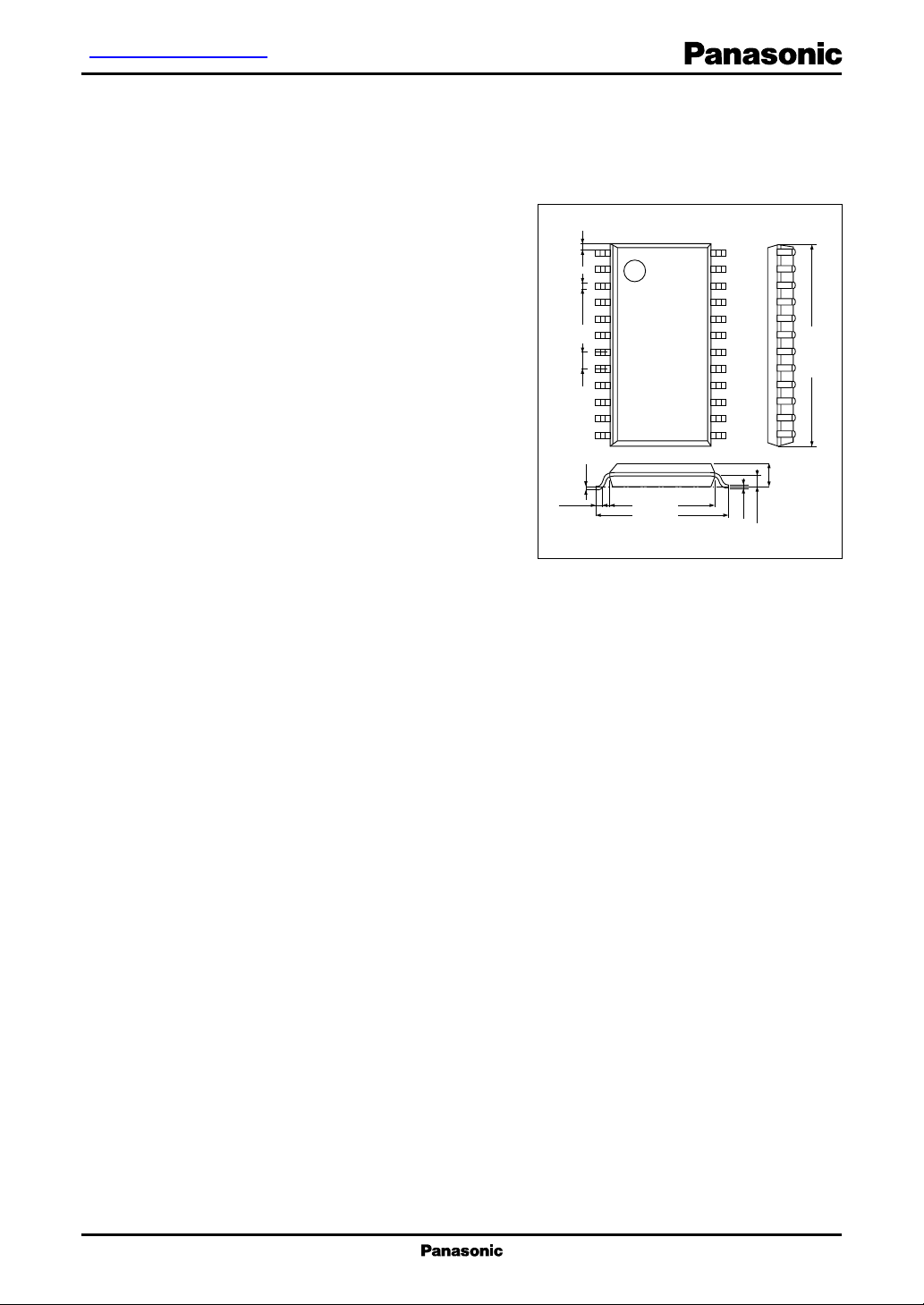
7.2±0.3
9.4±0.3
SOP024-P-0375A
Unit: mm
0.15
0.925
15.3±0.3
2.0±0.2
1
AN5829S ICs for T V
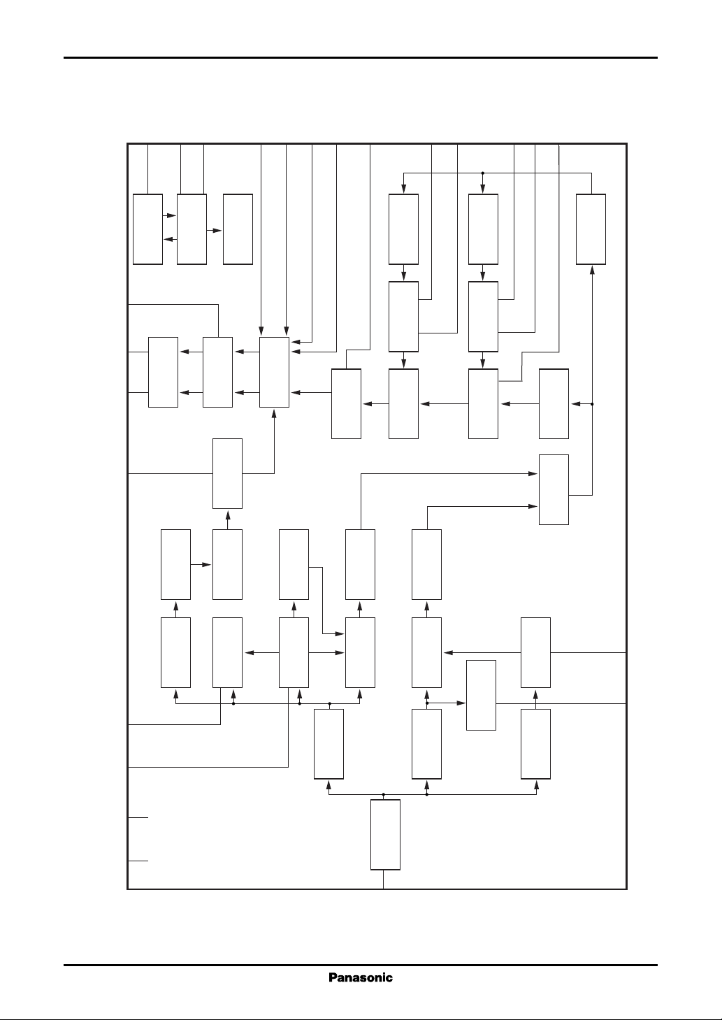
■ Block Diagram
R out
L out
1
22
21
4
20
PE
ZAP
Out SW
18
SCL
C
2
I
SDA
19
Decoder
AGC
Offset
24
DAC
cancel
AUX2 L
23
Matrix
AUX2 R
2
AUX1 L
3
AUX1 R
5
Offset
cancel
8
filter
Wide band
RMS det.
Wide band
expand
Wide band
6
11
filter
Spectral
Spectral
RMS det.
expand
Spectral
10
9
dbx
De-emph.
switch
(L−R)/SAP
H
, 2f
H
f
Trap filter
GND
V
CC
15
16
17
7
L+R
L+R
filter
demod
75 µs
De-emph.
Pilot det.
Pilot
cancel
St. PLL
filter
Stereo
L−R
L−R
filter
demod
Input VCA
14
MPX in
filter
SAP out
SAP
demod
SAP
filter
SAP
det.
det.
Noise
filter
Noise
12
13
2
ICs for TV AN5829S
■ Pin Descriptions
Pin No. Description
1 AGC timing
2 External input 1 L-ch
3 External input 1 R-ch
4 75 µs filter offset cancel
5 dbx offset cancel
6 Wideband timing
7V
CC
8 Wideband level sensor input
9 Spectral filter
10 Spectral timing
11 Spectral level sensor input
12 SAP noise level detection
■ Absolute Maximum Ratings
Parameter Symbol Rating Unit
Supply voltage V
Supply current I
Power dissipation
Operating ambient temperature
Storage temperature
Note)
The use of this IC, which builds in dbx-TV noise reduction, requires a license agreement with THAT Corporation.
1: Except fot the operating ambient temperature and storage temperature, all ratings are for Ta = 25°C.
*
2: Ta = 75°C
*
*2
1
*
*1
CC
CC
P
D
T
opr
T
stg
Pin No. Description
13 SAP carrier detection
14 Composite input
15 Pilot signal detection
16 Stereo PLL filter
17 GND
18 SCL
19 SDA
20 PE for ZAP
21 L-ch output
22 R-ch output
23 External input 2 R-ch.
24 External input 2 L-ch.
6.0 V
25 mA
150 mW
−20 to +75 °C
−55 to +125 °C
■ Recommended Operating Range
Parameter Symbol Range Unit
Supply voltage V
CC
4.5 to 5.5 V
3
AN5829S ICs for T V
■ Electrical Characteristics at VCC = 5 V, NR: On,Ta = 25°C
Input level (at 100% modulation) L+R: 75 mV[rms] (pre-emphasis off)
L−R: 150 mV[rms] (dbx noise reduction off)
Pilot: 15 mV[rms]
SAP: 45 mV[rms] (dbx noise reduction off)
Parameter Symbol Conditions Min Typ Max Unit
Total circuit current I
Mono output level V
Mono frequency characteristics-1
Mono frequency characteristics-2
Mono distortion ratio
Mono noise level V
(L), (R) output voltage difference
0(MON)
V
1(MON)
V
2(MON)
THD
N(MON)
V
LR(MON)
Stereo output level V
Stereo frequency characteristics-1
Stereo frequency characteristics-2
Stereo frequency characteristics-3
V
V
V
Stereo distortion ratio THD
Stereo noise level V
Stereo discrimination level V
Stereo discrimination hysteresis V
SAP output level V
SAP frequency characteristics-1 V
SAP frequency characteristics-2 V
SAP distortion ratio
SAP noise level V
SAP discrimination level V
SAP discrimination hysteresis V
N(ST)
TH(ST)
HY(ST)
0(SAP)
1(SAP)
2(SAP)
THD
N(SAP)
TH(SAP)
HY(SAP)
SAP → Stereo crosstalk C
Stereo → SAP crosstalk C
SAP → Mono crosstalk C
Mono → SAP crosstalk C
AUX 1, AUX 2 to INT C
crosstalk
INT, AUX 2 to AUX 1 C
crosstalk EXT: f = 1 kHz, 500 mV[rms]
INT, AUX 1 to AUX 2 C
crosstalk EXT: f = 1 kHz, 500 mV[rms]
No signal 11 18 25 mA
CC
f = 1 kHz, (mono) 100%mod 430 480 5 3 0
mV[rms]
f = 300 Hz, (mono) 30%mod − 0.5 0 0.5 dB
f = 8 kHz, (mono) 30%mod −1.2 − 0.1 0.7 dB
f = 1 kHz, (mono) 100%mod 0.7 %
(MON)
Input short-circuit, BPF (A curve) −60 dBV
f = 1 kHz, (mono) 100%mod − 0.5 0 0.5 dB
f = 1 kHz, (L(R)-only) 100%mod 380 480 580
0(ST)
f = 300 Hz, (L(R)-only) 30%mod − 0.7 0 0.7 dB
1(ST)
f = 3 kHz, (L(R)-only) 30%mod −10 1 dB
2(ST)
f = 8 kHz, (L(R)-only) 30%mod −2.5 − 0.5 1.5 dB
3(ST)
f = 1 kHz, (L(R)-only) 100%mod 1%
(ST)
mV[rms]
f = 15.73 kHz, (fH), 15 mV[rms] −60 dBV
fH, 2 fH Trap+BPF
f = 15.73 kHz (fH)4813
mV[rms]
f = 15.73 kHz (fH) 0.5 5dB
f = 1 kHz, (SAP) 100%mod 370 500 6 8 0
mV[rms]
f = 300 Hz, (SAP) 30%mod −10 1 dB
f = 3 kHz, (SAP) 30%mod −2.5 − 0.5 1 dB
f = 1 kHz, (SAP) 100% 1.5 %
(SAP)
f = 78.7 kHz, (5fH),V= 45 mV[rms], BPF
f = 78.7 kHz, (5fH)11 26
−70 dBV
mV[rms]
f = 78.7 kHz, (5fH) 0.5 5dB
(SAP)1 kHz, 100%mod −50 dB
T1
(Stereo) pilot-signal
(Stereo) 1 kHz, 100%mod −50 dB
T2
(SAP) carrier-signal
(SAP) 1 kHz, 100%mod −50 dB
T3
(Mono) 1 kHz, 100%mod −56 dB
T4
(SAP) carrier-signal
f = 1 kHz, VIN = 500 mV[rms] 50 dB
T5
INT: (mono) 1 kHz, 100%mod 50 dB
T6
INT: (mono) 1 kHz, 100%mod 50 dB
T7
4
ICs for TV AN5829S
■ Electrical Characteristics at VCC = 5 V, NR: On,Ta = 25°C (continued)
Parameter Symbol Conditions Min Typ Max Unit
1
AGC gain 1
AGC gain 2
I2 C interface
Sink current at ACK I
SCL, SDA signal input high level
SCL, SDA signal input low level
Input available maximum frequency
Note)*1: 00H register: D7 = 0, D6 = 1
• Design reference data
Note) The characteristics listed below are theoretical values based on the IC design and are not guaranteed.
Stereo separation (100%)-1 Sep
Stereo separation (100%)-2 Sep
Stereo separation (100%)-3 Sep
Stereo separation (100%)-4 Sep
Stereo separation (30%)-1 Sep
Stereo separation (30%)-2 Sep
Stereo separation (30%)-3 Sep
Stereo separation (30%)-4 Sep
Stereo separation (10%)-1 Sep
Stereo separation (10%)-2 Sep
Stereo separation (10%)-3 Sep
Stereo separation (10%)-4 Sep
I2 C interface
Bus free before start t
Start condition set-up time t
Start condition hold time t
Low period SCL, SDA t
High period SCL t
Rise time SCL, SDA t
Fall time SCL, SDA t
Data set-up time (write) t
Data hold time (write) t
Acknowledge set-up time t
Acknowledge hold time t
Stop condition set-up time t
*
1
*
V
V
AGC1
AGC2
ACK
V
V
f
Imax
f = 1 kHz, V
f = 1 kHz, V
= 50 mV[rms] 67 100 140
IN(EXT)
= 500 mV[rms] 180 2 70 390
IN(EXT)
Maximum pin 2 sink current at ACK 1 2 20 mA
3.5 5.0 V
IHI
0 0.9 V
ILO
100 kbit/s
mV[rms]
mV[rms]
Parameter Symbol Conditions Min Typ Max Unit
f = 300 Hz, (L(R)-only) 100%mod 20 35 dB
100-1
f = 1 kHz, (L(R)-only) 100 %mod 17 28 dB
100-2
f = 3 kHz, (L(R)-only) 100%mod 20 35 dB
100-3
f = 8 kHz, (L(R)-only) 100%mod 10 18 dB
100-4
f = 300 Hz, (L(R)-only) 30%mod 22 35 dB
30-1
f = 1 kHz, (L(R)-only) 30%mod 20 35 dB
30-2
f = 3 kHz, (L(R)-only) 30%mod 22 35 dB
30-3
f = 8 kHz, (L(R)-only) 30%mod 14 22 dB
30-4
f = 300 Hz, (L(R)-only) 10%mod 20 35 dB
10-1
f = 1 kHz, (L(R)-only) 10%mod 20 35 dB
10-2
f = 3 kHz, (L(R)-only) 10%mod 20 30 dB
10-3
f = 8 kHz, (L(R)-only) 10%mod 14 22 dB
10-4
BUF
SU.STA
HD.STA
SU.DAT
HD.DAT
SU.ACK
HD.ACK
SU.STO
4.0 µs
4.0 µs
4.0 µs
4.0 µs
LO
4.0 µs
HI
1.0 µs
r
0.35 µs
f
0.25 µs
0.3 µs
3.5 µs
0 µs
4.0 µs
5
AN5829S ICs for T V
■ Electrical Characteristics at VCC = 5 V, NR: On,Ta = 25°C (continued)
Start
condition
SDA
SCL
t
BUF
t
SU.DAT
Slave
address
t
HD.DAT
ACK ACK ACK
Sub
address
Data
byte
t
SU.STO
Stop
condition
t
LO
t
SU.STAtHDSTAtrtf
t
t
HI
LO
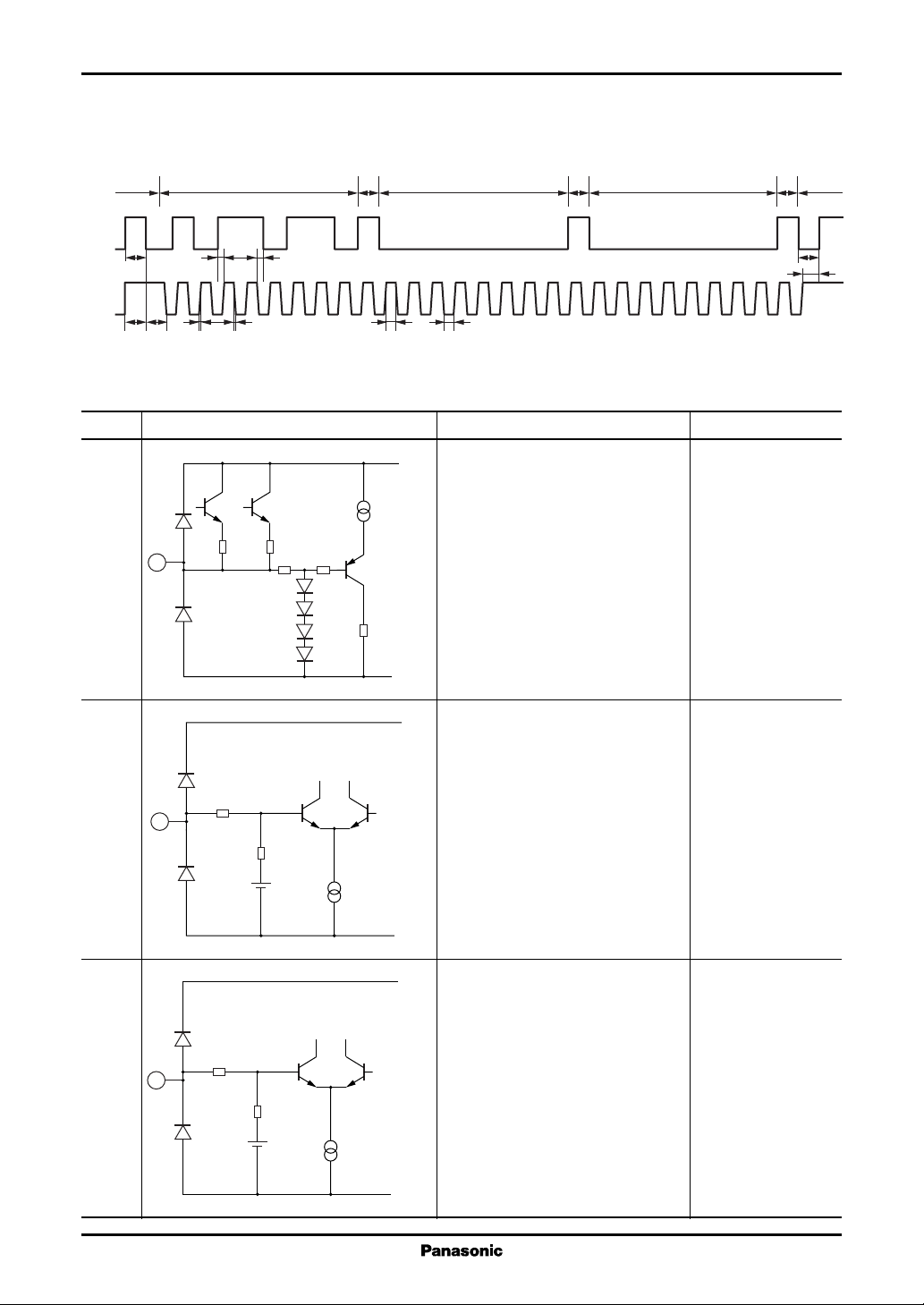
■ Terminal Equivalent Circuits
Pin No. Equivalent circuit Description DC voltage (V)
1 AGC: 0.5 to 2.0
51 kΩ
1
425 Ω
500 Ω
2 AUXIL: 2.2
2
20.7 kΩ
13.8 kΩ
V
CC
AGC level sensor pin
GND
V
CC
External input1
L-ch input pin
2.2 V
GND
3 AUXIR: 2.2
V
CC
External input 1
R-ch input pin
3
20.7 kΩ
13.8 kΩ
2.2 V
GND
6

ICs for TV AN5829S
■ Terminal Equivalent Circuits (continued)
Pin No. Equivalent circuit Description DC voltage (V)
4 OFCAN1: 2.2
524 Ω
4
80 kΩ
80 kΩ
2.2 V
V
CC
75 µs filter output
Offset cancel pin
GND
5 OFCAN2: 2.2
V
CC
dbx output
Offset cancel pin
524 Ω
5
80 kΩ
80 kΩ
2.2 V
GND
6 WBTIME: 2.2
7.5 µΑ
V
CC
Wide expander effective value detection
recovery time set-up pin
6
29 Ω
29 Ω
15 µΑ
GND
7 VCC: VCC pin V
8 WBDET: 2.2
V
CC
RMS detection circuit input pin
of wide band expander
8
14.4 kΩ
2.2 V
GND
CC
7

AN5829S ICs for T V
■ Terminal Equivalent Circuits (continued)
Pin No. Equivalent circuit Description DC voltage (V)
9 SPEFIL: 2.2
230 Ω
230 Ω
9
18 kΩ
2.2 V
18 kΩ
V
CC
Variable de-emphasis level adjusting
pin
GND
10 SPETIME: 0.2
7.5 µΑ
10
29 Ω
29 Ω
15 µΑ
V
CC
RMS detection recovery time pin of
variable de-emphasis
GND
11 SPEDET: 2.2
V
CC
RMS detection circuit input pin of
variable de-emphasis
11
3.2 kΩ
2.2 V
GND
12 NOISEDET: VCC − 2 V
V
CC
Noise detecting pin of SAP malfunction-prevention-circuit(Mute SAP demodulation at detecting noise.)
141 kΩ
12
BE
GND
8

ICs for TV AN5829S
■ Terminal Equivalent Circuits (continued)
Pin No. Equivalent circuit Description DC voltage (V)
13 SAPDET: V
163 kΩ
13
V
CC
SAP signal carrier level detection pin
GND
CC
− 2 V
BE
14 MPXIN: 2.2
14
524 Ω
54.4 kΩ
2.2 V
15 PILOTDET: 2.2VCC − 2 V
136 kΩ
15
V
CC
Composite signal input pin
GND
V
CC
Stereo pilot signal detection pin
GND
BE
16 PLL: VCC − 2 V
V
CC
Stereo PLL low pass filter connection
pin
58 kΩ
16
GND
17 GND: GND pin 0
BE
9

AN5829S ICs for T V
■ Terminal Equivalent Circuits (continued)
Pin No. Equivalent circuit Description DC voltage (V)
18 SCL:
51 kΩ
V
CC
I2C bus clock input pin
18
19 SDA: 2.2
19
20 PE:
20
1.7 kΩ
1.7 kΩ
51 kΩ
GND
V
CC
I2C bus data input pin
GND
Current application input pin for ZAP
at final test
GND
21 L-OUT: 2.2
520 Ω
21
430 Ω
850 Ω
2.2 V
GND
V
CC
L-ch. line out output pin
10

ICs for TV AN5829S
■ Terminal Equivalent Circuits (continued)
Pin No. Equivalent circuit Description DC voltage (V)
22 R OUT: 2.2
520 Ω
22
430 Ω
850 Ω
23 AUX2R: 2.2
23
20.7 kΩ
13.8 kΩ
2.2 V
GND
V
CC
R-ch. line out output pin
External input 2
V
CC
L-ch. input pin
2.2 V
GND
24 AUX2L: 2.2
V
External input 2
CC
R-ch. input pin
24
20.7 kΩ
13.8 kΩ
2.2 V
GND
11

AN5829S ICs for T V
■ Usage Notes
1. AGC set-up method
By turning on AGC, the AGC performs 0 dB at a small signal input, Boost at a medium signal and gain reduction
at a big signal. It can also control the I/O characteristics of AGC by I
2
C as shown below:
1 V
"00"
100 mV
10 mV
Output level (rms)
1 mV
1 mV
10 mV
2. Guarantee of I
2
C bus control operation at an operating ambient temperature is theoretially guranteed based on IC design by means
I
2
C operating temperature
of the inspection using about 50% faster clock speed at the normal temperature (T
AGC = Off
"11"
AGC = On
"01"
"10"
Data of sub
address 00H
100 mV 1 V 10 V
Input level (rms)
D7 D6
= 25°C).
a
Namely it is a theoretical value based on IC design, therefore it is not guranteed at the shipping inspection because
the inspection under a high and low temperature is not conducted.
3. Electrostatic breakdown
Pay attention to the following levels:
Pin 6: 200 pF, 130 V
Pin 10: 200 pF, 150 V
Pin 22: 200 pF, 190 V
AGC characteristics
12

ICs for TV AN5829S
■ Technical Information
[1] I2C bus
1. Receiving mode
SDA
SCL
Start
condition
1011
As transfer messages, SCL and SDA are transfered synchronouslly and serially. SCL is a constant clock
frequency and SDA is address data for controlling a receiving side and is sent in parallel by synchronizing with
SCL. Data are in principle sent by 8-bit 3-octet (byte) and there exists an acknowledge bit per octet. The frame
structure is mentioned below:
1) Start condition
When SDA becomes from high to low at SCL = high, the receiver gets ready to receive.
2) Stop condition
When SDA becomes from low to high at SCL = high, the receiver stops receiving.
3) Slave address
Specified for each device. If any addresses of other devices are sent, receiving will be stopped.
4) Sub-address
Specified for each function.
5) Data
Data for controlling
6) Acknowledge bit
This is the bit that informs the master of data reception every octet. The master sends the high signal and
the receiver sends back the low signal as shown with the dotted line in the above figure, thus the master
acknowledges reception on the receiver side. If the low signal is not sent back, the reception will be stopped.
Slave
address
B
Acknowledge
0110
6
bit
0000
Transmission message
Sub
address
0
Acknowledge
0010
2
bit
1000
Data Stop
8
Acknowledge
bit
0000
0
condition
Except for the start and stop conditions, SDA does not change at SCL = high.
13

AN5829S ICs for T V
■ Technical Information
[1] I2C bus (continued)
1. Receiving mode (continued)
2
C of this IC>
<I
1) Enhances adjustment-free mechanism of the TV set thanks to DAC control 3 and 9 switches
2) Auto-increment function
• Sub address 0
(Data sequential transfer leads to the sequential change of sub address, so that the data is inputted.)
• Sub address 8
(With sequential data transfer, data are inputted in the same sub address.)
2
3) I
C bus protocol
• Slave address
• Format (normal)
S Slave address A Sub address A Data byte A P
*
: Auto-increment mode
*
: Data renewal mode
W
Start
condition
Acknowledge bit
Write Mode: 0
Stop
condition
• Auto-increment mode/data renewal mode
S Slave address AW Sub address A Data 1 A Data 2 A A PData n
4) As the initial state of DAC is not guaranteed, never fail to input the following data in a power on mode.
"06" register: "04"
"00" register: adjustment data
"01" register: adjustment data
"02" register: "00"
"05" register: adjustment data
2. Transmission mode (read mode)
2
I
C bus protocol
• Slave address: 10110111 (B7H)
• Format
S Slave address A Data byte A P
R
Read
Mode: 1
14

ICs for TV AN5829S
■ Technical Information (continued)
[1] I2C bus (continued)
• Sub address byte and data byte format
Write mode (slave add.: 10110110)
Sub
address
D7 D6 D5 D4
Data byteUpper MSB Lower LSB
D3 D2 D1 D0
"00"
"01"
"02"
"05"
"06"
Read mode (slave add.: 10110111)
Upper MSB Lower LSB
D7 D6 D5 D4
Pilot det.
1 → DET
AGC adj. Input level adjustment
∗
∗
det.
AUX SW
0: Off
1: On
Mute: 1 → On
L: Mute
R: Mute
H
∗
∗
∗∗∗∗∗∗
AGC
1 → On
∗
∗
Data byte
High frequency separation adjustment
FMONO: 1 → On
0
∗
∗∗∗000
D3 D2 D1 D0
L: L+R
R: L+R
Low frequency separation adjustment
AUXselect
0: AUX1
1: AUX2
Adj.: 1 → On
L:
VGA out
R:
VCO f
SAP
1 → DET
St/SAP
0 → SAP
∗ = Don't care
(L+R)/SAP
0 → SAP
∗ = Don't care
15

AN5829S ICs for T V
■ Technical Information (continued)
[2] Noise detecting operation in SAP receiving mode
MPX
in
14
Input
VCA
150 kHz BPF
75 µs
De-emph.
dbx
Decoder
Stereo
filter
5f
H
SAP
filter
Noise
filter
BPF
SAP
det.
Noise
det.
Matrix
L−R
filter
SAP out
filter
13
12
SAP det.
Noise det.
SW1
a
b
DC voltage
comparater
SW2
a
b
c
a
b
c
Decoder
Decoder
21
L out
22
R out
dbx
I2C
16
Pin 14 input "02" register
Pin 12, pin 13
DC voltage
Noise: Small "00" V12 > V
Noise: Large "00" V12 < V
SW1 SW2 I2C SAP det.
13
13
b c 3.5 V to 5 V SAP
a a 0 V to 0.9 V L+R
Pin 21, pin 22

ICs for TV AN5829S
■ Application Circuit Example
20
PE
18
SCL
19
)
a
AUX2 L
AUX2 R
AUX1 L
AUX1 R
SDA
4.7 µF
4.7 µF
4.7 µF
4.7 µF
4.7 µF
3
5
24
23
2
0.33 µF
10 µF(T
8
6
11
)
a
3.3 µF(T
0.1 µF
0.022 µF
9
10
R out
L out
4.7 µF
180 kΩ
4.7 µF
4.7 µF
2.2 µF
0.1 µF
1
22
21
4
15
ZAP
C
2
I
Out SW
L+R
filter
L+R
demod
Decoder
AGC
Offset
75 µs
Pilot det.
DAC
cancel
De-emph.
Matrix
Pilot
St. PLL
cancel
Offset
cancel
L−R
filter
L−R
demod
filter
Wide band
RMS det.
Wide band
expand
Wide band
SAP out
SAP
filter
demod
filter
Spectral
Spectral
RMS det.
expand
Spectral
det.
SAP
det.
Noise
dbx
De-emph.
switch
(L−R)/SAP
H
, 2f
H
f
Trap filter
12
13
0.1 µF
0.1 µF
V
CC
5 V
0.047 µF
16
17
7
filter
Stereo
4.7 µF
Input VCA
14
MPX in
SAP
filter
filter
Noise
17
 Loading...