

Panasonic AN5819K Datasheet
ICs for TV
AN5819K
Sound multiplex demodulator IC for TV in the North American market
■ Overview
The AN5819K is a single chip IC, which includes a
sound multiplex demodulator for Zenith TV system and
the dbx TV sound noise reduction function.
■ Features
• Stereo demodulation, SAP demodulation and dbx noise
reduction are integrated into a single chip
• Enabling various kinds of adjustment and mode
changeover thanks to I
• Built-in input volume (I
2
C bus
2
C control) for interface with
intermediate frequency processing IC
■ Applications
• TV and VCR for the North American market
(A licensing agreement with THAT Corporation is necessary in order to use this IC with built-in dbx-TV noise
reduction function.)
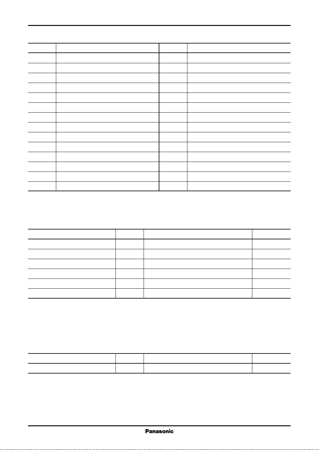
■ Block Diagram
9 V
CC
GND
V
MPX in
11
12
8
Input
VCA
9
21
7
Stereo
filter
SAP
filter
Noise
filter
6
Pilot det. Matrix
St.PLL
L+R
demod.
L−R
demod.
SAP
SAP out
demod.
SAP
noise
det.
V-reg.
I-reg.
13
14
28
27
10
L+R
filter
L−R
filter
filter
de-emph.
(L−R)/SAP
switch
15
17
75 µs
26.7±0.3
3° to 15°
1
2
3
4
5
6
7
8
9
10
11
12
13
14
8.4±0.3
10.16±0.25
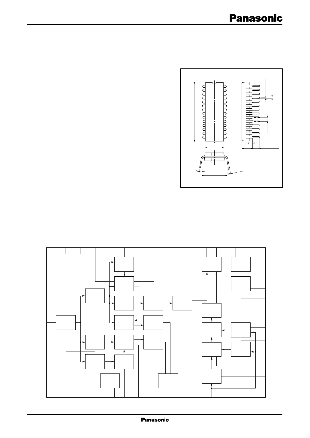
SDIP028-P-0400B
L-out
26
25
dbx
de-emph. 2
dbx
wide band
dbx
spectral
dbx
de-emph. 1
16
R-out
28
27
26
25
24
23
22
21
20
19
18
17
16
15
+0.1
–0.05
0.3
Stereo
5
LED
driver
decoder
Wide band
filter
Spectral
filter
4.8±0.25
4
I2C
SAP
Unit: mm
0.5±0.1
1.778
1.05±0.25
3.05±0.25
2
SDA
3
SCL
1
I2C
GND
22
23
20
19
18
24
0.9±0.25
1
AN5819K ICs for T V
■ Pin Descriptions
Pin No. Description
1I
2
C GND
2 SDA
3 SCL
4 SAP LED
5 Stereo LED
6 Pilot signal detection
7 Stereo PLL filter
8V
CC
9 SAP trap filter
10 Quasi sine-wave filter
11 Stereo filter offset cancel
12 Composite input
13 dbx timing current
14 Reference voltage source filter
Pin No. Description
15 (L−R)/SAP demodulation output
16 dbx input
17 (L+R) demodulation output offset cancel
18 Spectral level adjustment
19 Spectral timing
20 Spectral level sensor input
21 GND
22 Wide band level sensor input
23 Wide band timing
24 dbx offset cancel
25 R output
26 L output
27 SAP carrier detection
28 SAP noise level detection
■ Absolute Maximum Ratings
Parameter Symbol Rating Unit
Supply voltage V
Supply current I
3
LED drive current
Power dissipation
Operating ambient temperature
Storage temperature
Note)*1: Except for the operating ambient temperature and storage temperature, all ratings are for Ta = 25°C.
2: Power dissipation shown is for the IC package in free air at Ta = 70°C
*
3: LED drive currents are the currents flowing into pin 4 and pin 5.
*
*
2
*
1
*
1
*
I
T
T
CC
CC
LED
P
opr
stg
D
11.0 V
75 mA
10 mA
1 143 mW
−20 to +75 °C
−55 to +150 °C
■ Recommended Operating Range
Parameter Symbol Range Unit
Supply voltage V
CC
8.5 to 9.5 V
2
ICs for TV AN5819K
■ Electrical Characteristics at VCC = 9.0 V, Ta = 25°C
• Stereo PLL VCO adjustment: 15.734 kHz ± 50 Hz
• Input level (at 100% modulation)
L+R: 0.424 V[p-p] (pre-emphasis off)
L−R: 0.848 V[p-p] (dbx noise reduction off)
Pilot: 0.084 V[p-p]
SAP: 0.254 V[p-p] (dbx noise reduction off)
Parameter Symbol Conditions Min Typ Max Unit
Total circuit current I
Mono output level V
Mono frequency characteristics-1
Mono frequency characteristics-2
Mono distortion ratio
Mono noise level V
(L), (R) output voltage difference
0(MON)
V
1(MON)
V
2(MON)
THD
N(MON)
V
LR(MON)
Stereo output level V
Stereo frequency characteristics-1
Stereo frequency characteristics-2
Stereo frequency characteristics-3
V
V
V
Stereo distortion ratio THD
Stereo noise level V
Stereo discrimination level V
Stereo discrimination hysteresis V
SAP output level V
SAP frequency characteristics-1 V
SAP frequency characteristics-2 V
SAP distortion ratio
SAP noise level V
SAP discrimination level V
SAP discrimination hysteresis V
N(ST)
TH(ST)
HY(ST)
0(SAP)
1(SAP)
2(SAP)
THD
N(SAP)
TH(SAP)
HY(SAP)
SAP → Stereo crosstalk CT
Stereo → SAP crosstalk CT
Noise discrimination level V
Noise discrimination hysteresis V
TH(NOI)
HY(NOI)
No signal 35 55 75 mA
CC
f = 1 kHz, (mono) 100%mod. 480 530 580
f = 300 Hz, (mono) 30%mod. − 0.5 0 +0.5 dB
f = 8 kHz, (mono) 30%mod. −1.5 − 0.4 +0.4 dB
f = 1 kHz, (mono) 100%mod. 0.7 %
(MON)
Input short-circuit, BPF (A curve) −60 dBV
f = 1 kHz, (mono) 100%mod. − 0.5 0 +0.5 dB
f = 1 kHz, (L(R)-only) 100%mod. 420 520 620
0(ST)
f = 300 Hz, (L(R)-only) 30%mod. − 0.7 0 +0.7 dB
1(ST)
f = 3 kHz, (L(R)-only) 30%mod. −10+1dB
2(ST)
f = 8 kHz, (L(R)-only) 30%mod. −2.5 − 0.5 +1.5 dB
3(ST)
f = 1 kHz, (L(R)-only) 100%mod. 1%
(ST)
f = 15.73 kHz, (fH), V= 0.084 V[p-p], BPF
−60 dBV
f = 15.73 kHz (fH) 9 17 26
f = 15.73 kHz (fH) −6 − 0.5 dB
f = 1 kHz, (SAP) 100%mod. 350 500 7 00
f = 300 Hz, (SAP) 30%mod. −1.0 0 +1.0 dB
f = 3 kHz, (SAP) 30%mod. −3 −1.5 +0.5 dB
f = 1 kHz, (SAP) 100% 1.5 %
(SAP)
f = 78.7 kHz, (5fH),V= 0.42 V[p-p], BPF
−65 dBV
f = 78.7 kHz, (5fH)22 53
f = 78.7 kHz, (5fH) −4 − 0.5 dB
(SAP) 1 kHz, 100%mod. −50 dB
1
(Stereo) pilot-signal
(Stereo) 1 kHz, 100%mod. −50 dB
2
(SAP) carrier-signal
Pin 27: f
Pin 27: f
=
240 kHz at 5 V applied 38 84
=
240 kHz at 5 V applied −5.5 − 0.3 dB
mV[rms]
mV[rms]
mV[rms]
mV[rms]
mV[rms]
mV[rms]
3
AN5819K ICs for T V
■ Electrical Characteristics at VCC = 9.0 V, Ta = 25°C (continued)
Parameter Symbol Conditions Min Typ Max Unit
I2C interface
Sink current at ACK I
SCL, SDA signal input high level
SCL, SDA signal input low level
Input available maximum frequency
ACK
V
V
f
IMAX
• Design reference data
Note) The characteristics listed below are theoretical values based on the IC design and are not guaranteed.
Parameter Symbol Conditions Min Typ Max Unit
Stereo separation (30%)-1 Sep
Stereo separation (30%)-2 Sep
Stereo separation (30%)-3 Sep
Stereo separation (30%)-4 Sep
Stereo separation (100%)-1 Sep
Stereo separation (100%)-2 Sep
Stereo separation (100%)-3 Sep
Stereo separation (100%)-4 Sep
Stereo separation (10%)-1 Sep
Stereo separation (10%)-2 Sep
Stereo separation (10%)-3 Sep
Stereo separation (10%)-4 Sep
SAP → Mono crosstalk CT
Mono → SAP crosstalk CT
I2C interface
Bus free before start t
Start condition set-up time t
Start condition hold time t
BUF
SU.STA
HD.STA
Low period SCL, SDA t
High period SCL t
Rise time SCL, SDA t
Fall time SCL, SDA t
Data set-up time (write) t
Data hold time (write) t
SU.DAT
HD.DAT
Maximum pin-2 sink current at ACK 2.0 10 20 mA
3.5 5.0 V
IHI
0 0.9 V
ILO
100 kbit/s
f = 300 Hz, (L(R)-only) 30%mod. 22 30 dB
30-1
f = 1 kHz, (L(R)-only) 30%mod. 22 30 dB
30-2
f = 3 kHz, (L(R)-only) 30%mod. 22 30 dB
30-3
f = 8 kHz, (L(R)-only) 30%mod. 12 18 dB
30-4
f = 300 Hz, (L(R)-only) 100%mod. 20 30 dB
100-1
f = 1 kHz, (L(R)-only) 100%mod. 20 25 dB
100-2
f = 3 kHz, (L(R)-only) 100%mod. 20 30 dB
100-3
f = 8 kHz, (L(R)-only) 100%mod. 8 11 dB
100-4
f = 300 Hz, (L(R)-only) 10%mod. 20 30 dB
10-1
f = 1 kHz, (L(R)-only) 10%mod. 20 30 dB
10-2
f = 3 kHz, (L(R)-only) 10%mod. 20 30 dB
10-3
f = 8 kHz, (L(R)-only) 10%mod. 12 18 dB
10-4
(SAP) 1 kHz, 100%mod. −53 dB
3
(Mono)1 kHz, 0%mod.
(SAP) 1 kHz, 0%mod. −56 dB
4
(Mono) 1 kHz, 100%mod.
4.0 µs
4.0 µs
4.0 µs
4.0 µs
LO
4.0 µs
HI
1.0 µs
r
0.35 µs
f
0.25 µs
0 µs
4
 Loading...