

Panasonic AN5757S Datasheet
ICs for TV
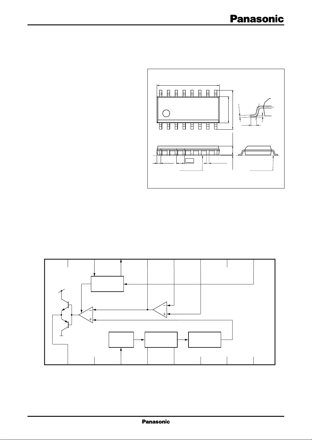
0.3
(0° to 10°)
(0.15)
10.1±0.3
4.2±0.3
6.5±0.3
18
16 9
1.27
(0.605)
Seating plane Seating plane
0.40±0.25
0.1±0.1 1.5±0.2
AN5757S
CRT horizontal deflection voltage control IC
■ Overview
The AN5757S is an IC for PWM-system CRT
horizontal deflection voltage control. It can be used
for horizontal frequency from 20 kHz to 140 kHz
and applicable from a popular type monitor to high
precision monitor. Its SO-16-pin package enables
the users to desigh the sets simple and efficient.
■ Features
• PWM output
• Built-in thermal protection circuit (cut off both
upper and lower push-pull output transistor)
• Soft start function
• Built-in error amp.
■ Applications
• CRT monitors
■ Block Diagram
Unit: mm
SOP016-P-0225A
GND2
16
V
CC2
GND2
1
15
2
SW1
CC2
V
DTC
V
14
Sync. in
3
CC1
HD in
13
Duty
adjustment
4
Control
12
5
11
Ramp
generator
6
N.C.
CC1
V
10
7
GND1
SW2
9
8
N.C.
1
AN5757S ICs for T V
■ Pin Descriptions
Pin No. Description
1 PWM output
2 Power supply for output (V
CC2
)
3 Horizontal synchronous input (HD in)
4 Duty adjustment (capacitor)
5 Duty adjustment (resistor)
6N.C.
7 GND1
8N.C.
■ Absolute Maximum Ratings
Parameter Symbol Rating Unit
Supply voltage V
Supply current I
Output current I
2
Power dissipation
Operating ambient temperature
Storage temperature
Note)*1: Except for the power dissipation, operating ambient temperature, and storage temperature, all ratings are for Ta = 25°C.
2: The power dissipation shown is for the IC package in free air at Ta = 70°C.
*
*
1
*
1
*
CC1
V
CC2
CC1
I
CC2
1
P
D
T
opr
T
stg
Pin No. Description
9 On/off SW input2 (SW2)
10 Power supply (V
CC1
)
11 IN+
12 IN−
13 NF
14 Capacitor for DTC
15 On/off SW input1 (SW1)
16 GND2
13.2 V
13.2
6.3 mA
15.0
±150 mA
198 mW
−20 to +70 °C
−55 to +125 °C
■ Recommended Operating Range
Parameter Symbol Range Unit
Supply voltage V
HD input V
SW1 input V
SW2 input V
Max. duty adjustment voltage V
Error amp. positive input V
Error amp. negative input V
Max. output current of PWM output I
Note) '+' denotes current flowing into the IC, and '−' denotes current flowing out of the IC.
HD input
PWM output
5 V
0 V
11.6 V
0.2 V
2
t
OUT
CC1
t
IN
, V
3
I15
I9
5
11
12
1(max)
CC2
11.0 to 13.0 V
0 to V
0 to V
0 to V
0 to 6 V
0 to 6 V
0 to 6 V
−150 to +150 mA
10
10
10
Minimum width (t
can be adjusted at pin 5.
Use it to get t
Output stops at t
OUT min
OUT min
OUT min
< t
) of the t
IN
≥ t
IN
V
V
V
OUT
ICs for TV AN5757S
■ Electrical Characteristics at Ta = 25°C
Parameter Symbol Conditions Min Typ Max Unit
Power supply current I
CC1
VCC = 12 V, V
V3 = 5 V, V11 = 0 V
Power supply current for output I
CC2
VCC = 12 V, V
V3 = 5 V, V11 = 0 V
Duty
Pin voltage of duty adjustment V
5−7VCC
= 12 V, 2.0 3.0 4.0 V
resistor pin V3 = 0 V
Pin current (for discharge) of duty 1
VCC = 12 V, 3.0 mA
4D
adjustment capacitor pin V3 = 0 V, V4 = 1 V
Pin current (for charge) of duty 1
VCC = 12 V, −60 −45 −30 µA
4C
adjustment capacitor pin V3 = 5 V, V4 = 1 V
High-level of duty adjustment V
4−7HVCC
= 12 V, 3.2 3.7 4.2 V
capacitor pin V3 = 5 V
Low-level of duty adjustment V
4−7LVCC
= 12 V, 0 0.15 V
capacitor pin V3 = 0 V
DTC
SW2 pin current H I
VCC = 12 V, V3 = 5 V, 200 300 400 µA
9H
V9 = 12 V
SW2 pin current M I
VCC = 12 V, V3 = 5 V, 45 70 95 µA
9M
V9 = 5 V
SW2 pin current L I
VCC = 12 V, V3 = 5 V, −5 0 µA
9L
V9 = 0 V
SW1 pin current H I
VCC = 12 V, V3 = 5 V, 200 300 400 µA
15H
V15 = 12 V
SW1 pin current M I
15MVCC
= 12 V, V3 = 5 V, 45 70 95 µA
V15 = 5 V
SW1 pin current L I
VCC = 12 V, V3 = 5 V, −5 0 µA
15L
V15 = 0 V
Pin current (discharge) of DTC I
capacitor pin V
Pin current (charge) of DTC I
capacitor pin V
High-level of DTC capacitor pin V
Low-level of DTC capacitor pin V
VCC = 12 V, V14 = 5 V, 60 90 120 µA
14D
= 12 V
9, 15
VCC = 12 V, V14 = 10 V, −15 −8 −1mA
14C
= 0 V
9, 15
14−7HVCC
14−7LVCC
= 12 V, 11.5 V
V
= 0 V
9, 15
= 12 V, 0 0.15 V
V
= 12 V
9, 15
= 5 V, 2.0 4.0 6.0 mA
9, 15
= 5 V, 6.0 10.0 14.0 mA
9, 15
3
 Loading...