

Panasonic AN5693K Datasheet

ICs for TV
AN5693K
Luminance,Chroma and Sync. Signals Processing IC(with Built-in I2Cbus Interface)for PAL/NTSC Color-TV
■ Overview
The AN5693K is an IC that processes PAL-and NTSCcompatible video,chroma,RGB and sync. signals.
■ Features
• Built-in I2C-bus control interface.
• SECAM-compatible together with the AN5637 SECAM
signal processing IC.
■ Applications
• TV(Multi-system compatible)
1
26 27
3 to 15˚ 3 to 15˚
52
47.7±0.3
13.7±0.3
(15.24)
SDIP052-P-0600A
Unit : mm
(0.7)
3.85±0.3
(3.3)
0.5±0.1
1.0±0.25
1.778
1
AN5693K ICs for T V
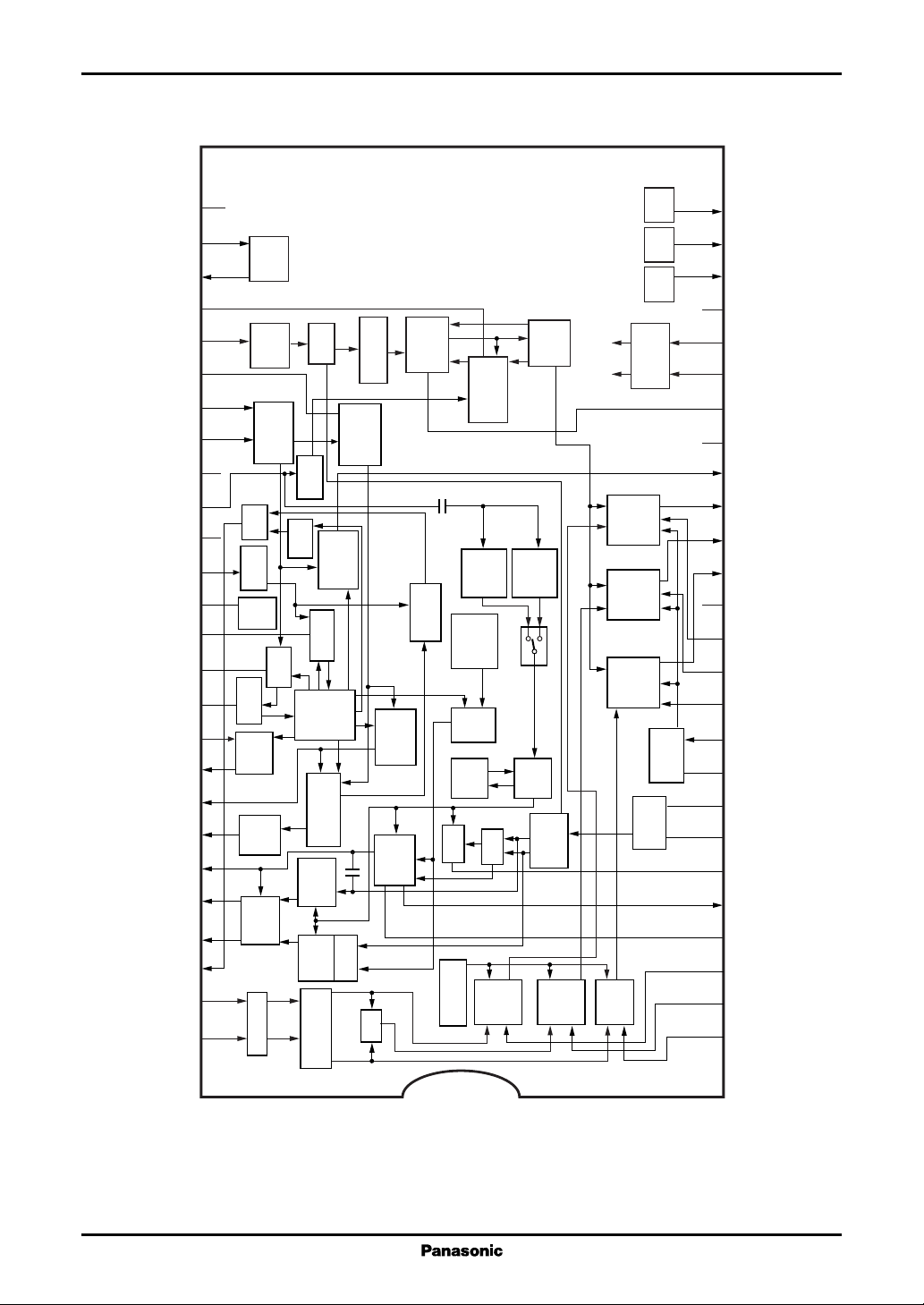
■ Block Diagram
N.C.
Video In
Video Out
BL Det.
Y In
Ver. Clamp
Ver. Sync. In
Hor. Sync. In
(VCJ)
V
CC3
5V
C In
GND(VCJ)
FBP In
V
CC2
AFC2
AFC1
Hor. VCO
X-ray
H-Out
50/60Hz Det. Out
V-Out
SECAM
−(B−Y)Out
−(R−Y)Out
SCP
−(B−Y)In
−(R−Y)In
27
*7-bit
28
SW
out
DAC
out
*9-bit
*7-bit
C bus
2
I
29
Video
adjust
*4-bit
30
(Service)
31
32
CV
*1-bit
clamp
Trap
*6-bit
*7-bit
Sharpness
Y
contrast
*1-bit
Y
clamp
33
Black
expansion
34
Hor.
35
sync. sep.
36
37
SCP
LPF
Ver.
sync. sep.
drive
B
BGP
38
Hor.
HBLK
39
Hor.
40
reg.
41
AFC1
lock det.
HVBLK
AFC2
*4-bit
42
HVCO
43
44
Shut
down
Hor.
count
down
50/60Hz
detect
45
46
out
Ver.
47
48
SW
PN/S
49
*1-bit
50
Ver.
B-Y
R-Y
count down
*2-bit
demod
+/−
demod
(50/60Hz)
Killer
ident
*1-bit
ACC
APC
BPF
PAL
SW
System
FF
1H
det.
Tint
BPF
NTSC
Chroma SW
*1-bit
amp.
ACC
*7-bit
generate
CW
G
R
*1-bit
cut off
drive
*Drive 8-bit
*Cut off 9-bit
Chroma
51
*8-bit
52
*7-bit
Saturation
contrast
Chroma
G-Y
B-Y
Brightness
clamp
G-Y
clamp
R-Y
clamp
Ext.
DAC3
Ext.
DAC2
Ext.
DAC1
interface
cut off
(8-bit)
cut off
YSpulse
VCO
26
Ext. DAC3
25
Ext. DAC2
24
Ext. DAC1
23
GND(Ext. DAC)
22
SCL
21
SDA
20
ACL
19
GND(RGB)
18
Lock Det.
17
B-Out
16
G-Out
15
R-Out
14
V
CC1
13
B-In
12
G-In
11
R-In
10
Y
S
9
Spot Killer
8
VCO 3.58MHz
7
VCO 4.43MHz
6
APC
5
Killer Out
4
Killer
3
B-Clamp
2
G-Clamp
1
R-Clamp
9V
2

ICs for TV AN5693K
■ Pin Descriptions
Pin No. Description
1(R−Y)Clamp
2(G−Y)Clamp
3(B−Y)Clamp
4 Killer Filter
5 Killer Output
6 Chroma APC Filter
7 Chroma VCO 4.43 MHz
8 Chroma VCO 3.58 MHz
9 Spot Killer
10 YS Input(Fast Blanking)
11 External R Input
12 External G Input
13 External B Input
14 V
CC1
15 R Output
16 G Output
17 B Output
18 Hor. Lock Detect
19 GND(RGB/I2C/DAC)
20 ACL
21 SDA
22 SCL
23 GND(EXT DAC)
24 External DAC 1 DC
25 External DAC 2 DC
26 External DAC 3 DC
Pin No. Description
27 N.C.
28 Video Level Adjust Input
29 Video Level Adjust Output
30 Black Level Det/Blank Off SW
31 Y Input
32 Ver. Sync. Clamp
33 Ver. Sync. Input
34 Hor. Sync. Input
35 V
(Chroma/Jungle/DAC)
CC3
36 Chroma Input/Black Exp. Start
37 GND(Video/Chroma/Jungle)
38 FBP Input
39 V
(Hor. Stability Supply)
CC2
40 Hor. AFC 2 Filter
41 Hor. AFC 1 Filter
42 Hor. VCO(32 fH)
43 X-Ray Protection Input
44 Hor.Pulse Output
45 Ver. 50/60 Hz Detect Output
46 Ver. Pulse Output
47 SECAM Interface/CW Output
48 −(B−Y)Output
49 −(R−Y)Output
50 Sandcastle Pulse Output
51 −(B−Y)Input
52 −(R−Y)Input
3

AN5693K ICs for T V
■ Absolute Maximum Ratings
Parameter Symbol Rating Unit
Power supply voltage V
Power supply current I
2
Power dissipation
Operating ambient temperature
Storage temperature
*
1
*
1
*
CC
CC
P
D
T
opr
T
stg
Note) *1: The temperature of all items shall be Ta = 25 °C, except storage temperature and operating ambient temperature.
*2: Power dissipation is at Ta = 70 °C(Refer to "Technical information")
■ Recommended Operating Range
Parameter Symbol Range Unit
Operating supply voltage range V
Operating supply pin voltage V
Do not apply voltage or current externally to any pin not listed in this table.
Note)
As for circuit current,(+)is the current flowing into the IC and(−)is the current flowing out of the IC.
CC1
V
CC3
5
V
9
V
10
V
11
V
12
V
13
V
21
V
22
V
24
V
25
V
36
V
38
V
43
V
45
V
47
V
(14) 10.5 V
CC1
V
(35) 6.0
CC3
I
14
I
35
I
39
77 mA
119
27
1 372 mW
−20 to +70 °C
−55 to +150 °C
8.1 to 9.9 V
4.5 to 5.5
0 to 6 V
0 to V
14
0 to 6
0 to 6
0 to 6
0 to 6
0 to 6
0 to 6
0 to V
14
0 to V
14
0 to V
14
0 to V
47
0 to 2
0 to 6
0 to V
14
4
ICs for TV AN5693K
■ Recommended Operating Range
Parameter Symbol Range Unit
Operating supply circuit current I
Do not apply voltage or current externally to any pin not listed in this table.
Note)
As for circuit current,(+)is the current flowing into the IC and(−)is the current flowing out of the IC.
39
I
15
I
16
I
17
I
28
I
29
I
33
I
34
I
44
I
46
I
47
10 to 25 mA
− 6.0 to + 0.6
− 6.0 to + 0.6
− 6.0 to + 0.6
− 0.3 to + 0.1
− 2.4 to + 0.8
− 0.8 to + 0.1
− 0.8 to + 0.1
− 6.4 to + 0.1
− 0.8 to + 0.1
− 0.3 to + 0.1
■ Electrical Characteristics at Ta = 25 °C
Parameter Symbol Conditions Min Typ Max Unit
Power supply DAC data is standard.
Supply current 1 I
Supply current 2 I
Steady state supply voltage V
Steady state supply Current I
Steady state supply input R
resistance I39 = 10 mA ∼ 25 mA
Interface
Video adjust gain V
Video adjust output resistance R
External DAC 1 DC voltage V
EXT1max
(max.) DC measurement
External DAC 1 DC voltage V
EXT1min
(min.) DC measurement
External DAC 2 DC voltage V
EXT2max
(max.) DC measurement
External DAC 2 DC voltage V
EXT2min
(min.) DC measurement
Current when V14 = 9 V 384858mA
14
Current when V35 = 5 V 486072mA
35
When Pin39 current 5.8 6.5 7.2 V
39
I = 15 mA,Pin39 voltage
Current when V39 = 5 V 2 5 7 mA
39
DC measurement input resistance when 1 5 10 Ω
39
PO
DC measurement 20 log
output(0A = 08)
DC measurement 70 120 170 Ω
O29
Pin24 DC voltage when DAC 0C = 00 3.10 3.40 3.70 V
Pin24 DC voltage when DAC 0C = 7F 2.10 2.40 2.70 V
Pin25 DC voltage DAC 0B = 00,04D7 = 0 7.8 8.1 8.7 V
Pin25 DC voltage DAC 0B = FF,04D7 = 1 0.1 0.8 1.0 V
output(0A = F8) 5 6 7 dB
5

AN5693K ICs for T V
■ Electrical Characteristics at Ta = 25 °C (continued)
Parameter Symbol Conditions Min Typ Max Unit
Interface(continued)
External DAC 3 DC voltage V
EXT3max
(max.) DC measurement
External DAC 3 DC voltage V
EXT3min
(min.) DC measurement
External DAC 1 maximum I
EXT1max
output current DC measurement
External DAC 3 maximum I
EXT3max
output current DC measurement
Video signal processing Input 0.6 VPP stair step. Measure at G-out(VWB = 0.42 VOP)
Video output(typ.) V
Video output(max.) V
Video output(min.) V
Contrast variable range Y
Cmax/min
Video frequency characteristics f
Sharpness variable range Y
Smax/min
Pedestal level(typ.) V
Pedestal variable range ∆V
Brightness control sensitivity ∆V
Video input clamp voltage V
ACL sensitivity ACL When V
Blanking off threshold voltage V
Blanking level V
DC transmission quantity T
Video input clamp current I
ACL start point V
Pin26 DC voltage when DAC 0D = 7F 5.50 6.00 6.50 V
Pin26 DC voltage when DAC 0D = 00 0.90 1.00 1.15 V
Pin24 DC current when DAC 0C = 7F 200 µA
Pin26 DC current when DAC 0D = 7F 1.0 mA
DAC 03 = 40(typ.),(Contrast) 1.65 2.10 2.55 V
YO
DAC 03 = 7F(max.),(Contrast) 3.60 4.50 5.35 V
YOmax
DAC 03 = 00(min.),(Contrast) 0.07 0.25 0.50 V
YOmin
DAC 03 = 7F,DAC 03 = 00 20 25 33 dB
f = 0.2 MHz as reference to −3 dB. 5.5 6.8 MHz
YC
DAC 0E D1 = 1,DAC 04 = 00(Sharp)
f = 3.8 MHz,DAC 0E D1 = 1 9 13 17 dB
Sharp : (04 3F)/(04 00)
DAC 02 = 80(typ.),(Brightness) 1.9 2.5 3.1 V
PED
Difference between DAC 02 = 00 & FF 2.0 2.6 3.2 V
PED
(Brightness)
Average variable range of DAC 02 = 60 & A 0 8 11 14 mV/step
BRT
Pin31 clamp voltage 3.2 3.7 4.2 V
YCLP
= 3.0 V−3.5 V 2 times of Y-out 2.1 2.7 3.2 V/V
20
increase
Reduse Pin30 voltage ; the voltage when 0.3 0.5 0 .9 V
BOFF
blanking is off
Blanking pulse DC voltage. 0.5 1.0 1.5 V
YBL
APL : 10 % to 90 %,TDC 9 100 110 %
DC
(∆AC − ∆DC)100 %
TDC
∆AC
DC measurement IC : internal sink current 8 13 18 µA
YCLP
ACL Pin20 voltage reduces from 5 V until 3.4 3.7 4.0 V
ACL
output is lesser by 10 %
PP
PP
PP
6

ICs for TV AN5693K
■ Electrical Characteristics at Ta = 25 °C (continued)
Parameter Symbol Conditions Min Typ Max Unit
Color signal processing All tests on : Burst 300 mVPP(PAL),typ. : B-out
Color difference output(typ.) V
Color difference output(max.) V
Color difference output(min.) V
Chroma contrast variable range C
Cmax/min
ACC.characteristics 1 ACC1 Input : Rainbow 0.9 1.0 1.2 Times
ACC.characteristics 2 ACC2 Input : Rainbow 0.7 1.0 1.1 Times
NTSC tint centre ∆θ
NTSC tint adjustable range 1 ∆θ
NTSC tint adjustable range 2 ∆θ
Demodulation output ratio(R) R/B Input : Rainbow 0.71 0.83 0.95 Times
PAL,NTSC Ratio of R-out/B-out
Demodulation output ratio(G) G/B Input : Rainbow 0.31 0.37 0.43 Times
PAL,NTSC Ratio of G-out/B-out
Color difference output angle ∠R Input : Rainbow 78 90 102 Deg
(R) PAL,NTSC
Color difference output angle ∠G Input : Rainbow 224 236 248 Deg
(G) PAL,NTSC
Color killer tolerance(PAL) V
Color killer tolerance(NTSC) V
APC pull-in range(H) f
PAL,NTSC High side pull-in range
APC pull-in range(L) f
PAL,NTSC Low side pull-in range
Color killer detector output V
voltage(Color) inputed
Color killer detector output V
voltage(B/W) inputed
Input : Color bar 2.6 3.3 4.0 V
COtyp
DAC 00 = 40(typ.),DAC 03 = 40(typ.)
Input : Color bar 2.3 3.0 V
COmax
DAC 00 = 7F,DAC 03 = 40
Input : Color bar 0 100 mV
COmin
DAC 00 = 00,DAC 03 =40
DAC 00 = 40,DAC 03 = 7F,DAC 03 = 00 20 25 33 dB
Burst increase from 300 mVPP → 600 mV
Burst decrease from 300 mVPP → 60 mV
Difference −13 0 13 Step
C
PP
PP
between DAC 01 = 40 & when tint is centre
Input : Rainbow,DAC 01 = 7F(Tint) 30 50 65 Deg
1
Input : Rainbow,DAC 01 = 00(Tint) −65 −50 −30 Deg
2
Input : Color bar,0 dB = 300 mV
KILLP
PP
−57 −44 −34 dB
Attenuate input level
Input : Color bar,0 dB = 300 mV
KILLN
PP
−57 −44 −34 dB
Attenuate input level
Input : Color bar 450 900 Hz
CPH
Input : Color bar −900 − 450 Hz
CPL
Voltage at Pin5 when chroma signal is 4.5 5.0 V
KC
Voltage at Pin5 when no chroma signal is 0 0.1 0.5 V
KBW
PP
OP
PP
7
AN5693K ICs for T V
■ Electrical Characteristics at Ta = 25 °C (continued)
Parameter Symbol Conditions Min Typ Max Unit
Color signal processing All tests on : Burst 300 mVPP(PAL)typ.: B-out (continued)
Demodulation output−(B−Y) V
PAL,NTSC centre)Measure Pin48
Demodulation output−(R−Y) V
PAL,NTSC centre)Measure Pin49
Demodulation output angle ∠R
∠B PAL,NTSC Phase difference of B−Y axis
Demodulation output angle ∠R
∠R PAL,NTSC Phase difference of B−Y and R−Y axis
CW output level(4.43 MHz) V
CW output level(3.58 MHz) V
SECAM output CW period T
SECAM detector current I
SECAM
PAL/NTSC output DC voltage V
SECAM output DC voltage V
Demodulation output R
O48,49PN
impedance(PAL/NTSC) mode
−(R−Y), −(B−Y)
Demodulation output R
O48,49S
impedance(SECAM) mode
−(R−Y), −(B−Y)
RGB processing DAC data standard
Pedestal difference voltage ∆V
Brightness voltage tracking ∆V
Video voltage gain ratio ∆G
Video voltage gain tracking ∆T
Driver control characteristics G
Cut-off control characteristics V
CUTOFF
YS threshold voltage V
Input : Color bar(NTSC : Adjust to tint 555 695 835 mV
DB
Input : Color bar(NTSC : Adjust to tint 430 540 650 mV
DR
Input : Rainbow −5 0 5 Deg
DB
Input : Rainbow 85 90 95 Deg
DR
AC component at Pin47 when VCO is at 250 300 350 mV
CWP
4.43 MHz
AC component at Pin47 when VCO is at 050mV
CWN
3.58 MHz
Period of CW is outputed when in SECAM 1.31 1.41 1.51 ms
CW
Minimum current from Pin47 when 50 100 150 µs
SECAM is detected
PAL/NTSC output DC voltage at Pin47 0.80 1.30 1.65 V
47PN
SECAM output DC voltage at Pin47 4.1 4.6 5.1 V
47S
Pin impadance of Pin48,49 in PAL/NTSC 390 480 570 Ω
Pin impadance of Pin48,49 in SECAM 1 0 0 kΩ
R,G,B out pedestal difference voltage 0 0.3 V
IPL
DAC 02 = 40 to C0(Brightness). 0.9 1.0 1.1 Times
BL
Ratio of variable level
R,B out output ratio with G-oth 0.8 1.0 1.2 Times
YC
DAC 03 = 20 to 60 ratio(contrast)of gain 0.9 1.0 1.1 Times
CONT
R,B out AC adj. amount 5.3 6.3 7.3 dB
DV
Driver DAC 08 = 00 to FF
Driver DAC 09 = 00 to FF
R,G,B output DC cut off DAC range from 1.9 2.4 2.9 V
min.to max.
Smallest level when YS is on 0.7 1.0 1.3 V
YS
PP
PP
PP
PP
Times
8
ICs for TV AN5693K
■ Electrical Characteristics at Ta = 25 °C (continued)
Parameter Symbol Conditions Min Typ Max Unit
RGB processing DAC data standard (continued)
External RGB DC Voltage V
External RGB pedestal ∆V
difference voltage(R/B)(G/B)
Internal/External pedestal ∆V
difference voltage
External RGB output Voltage V
External RGB output ∆V
difference voltage
External RGB contrast E
Cmax/min
control characteristics
External RGB frequency f
RGBC
characteristics
Synchronizing signal processing
Horizontal output free run f
frequency The frequency at Pin44
Horizontal output pulse duty τ
Horizontal output pull-in range f
Vertical free run frequency f
(PAL) D3 = 0,No sync.signal input
Vertical free run frequency f
(NTSC) D3 = 1,No sync.signal input
Vertical output pulse width τ
NTSC,PAL at Pin46
Vertical pull-in range(PAL) f
Vertical pull-in range(NTSC) f
Horizontal output voltage(H) V
Horizontal output voltage(L) V
Vertical output voltage(H) V
Vertical output voltage(L) V
Screen centre variable range ∆T
YS is on 1.7 2.3 2.9 V
EPL
EPLYS
PL/IE
ERGB
ERGB
is on 0 250 mV
Internal−External 50 200 400 mV
Input 3 VPP,DAC 03 = 7F(Contrast) 4.3 5. 4 6. 5 V
Input 3 VPP,DAC 03 = 7F(Contrast) − 0.6 0 + 0.6 V
DAC 03 = 7F,DAC 03 = 00 10 13 16 dB
Input 0.2 VPP,DC = 1 V 8 12 MHz
No input signal 15.33 15.63 15.93 kHz
HO
Horizontal output pulse's high level's 31 37 43 %
HO
duty
Horizontal sync. sep. freq. pull-in approach- ± 500 ± 650 Hz
HP
ing 15.625 kHz
Forced 50 Hz mode, DAC 0E-D2 = 1 485052Hz
VO-P
Forced 60 Hz mode, DAC 0E-D2 = 1 586062Hz
VO-N
Hor. & Ver.sync. condition,the pulse width 9 10 11 1/fH
VO
fH = 15.625 kHz,Forced 50 Hz mode 46 54 Hz
VPP
VPNfH
44H
= 15.75 kHz,Forced 60 Hz mode 56 64 Hz
Horizontal output pulse's high level's DC 3.2 3.5 3.8 V
voltage
Horizontal output pulse's low level's DC 0 0.3 V
44L
voltage
Vertical output pulse's high level's DC 3.9 4.2 4.5 V
46H
voltage
Vertical output pulse's low level's DC 0 0.3 V
46L
voltage
Variable amount of phase between H
HC
& H
DAC 0A = 80 to 8F
OUT
2.6 3.2 4.4 µs
SYNC
PP
9
AN5693K ICs for T V
■ Electrical Characteristics at Ta = 25 °C (continued)
Parameter Symbol Conditions Min Typ Max Unit
Synchronizing signal processing(continued)
Shut down operating V
Vertical frequency f
detection operation(50 Hz) Pin45 = "L"(< 0.5 V)
Vertical frequency f
detection operation(60 Hz) Pin45 = "H"(> 4.5 V)
Sync. separation input clamp V
voltage(Vertical)
Sync. separation input clamp V
voltage(Horizontal)
Horizontal output start voltage V
I2C interface
Sinking current at ACK I
SCL,SDA signal input high V
level
SCL,SDA signal input low V
level
Input possible maximum f
frequency
Pin43 minimum voltage when H-out does 0.60 0.68 0.76 V
43L
not appear
Vertical input freq.when the DC level at 47 55 Hz
50
Vertical input freq. when the DC level at 57 63 Hz
60
V33 clamp voltage 1.0 1.3 1.6 V
33
V34 clamp voltage 1.0 1.3 1.6 V
34
Minimum V38 when horizontal output is 3.4 4.2 5. 0 V
fHS
above 1 VPP,fo > 10 kHz
When ACK,Pin21 pin current with 2.2 kΩ 1.8 2.5 5.0 mA
ACK
pull-up to 5 V
IHI
ILO
Imax
3.1 5.0 V
0 0.9 V
100 Kbit/s
• Reference data for design
The characteristic values below are theoretical values for designing and not guaranteed.
Note)
Parameter Symbol Conditions Min Typ Max Unit
Video signal processing (VWB = 0.42 VOP) Input 0.6 VPP stair step. Measure at G-out
Y signal delay time t
Measure output's delay time with input 620 6 90 760 ns
DL
(PAL = 4.43 MHz)
Black level correction 1 V
All black input. Find the diff.of G-out when −100 0 +100 mV
BLC1
Pin30 is 9 V & open
Black level correction 2 V
All black input. Find the diff.of G-out when 500 800 1100 mV
BLC2
Pin30 is 3 V & 9 V
Black level correction 3 V
Input : About 20 IRE the diff.of G-out when 100 300 500 mV
BLC3
Pin30 is open & 9 V
Contrast variation with ∆V
Y-out output level difference when −300 0 +300 mV
CS
sharpness sharpness = max. to min.
Brightness variation with ∆V
Pedestal DC level difference when −250 0 +250 mV
BS
sharpness sharpness = max. to min.
10
ICs for TV AN5693K
■ Electrical Characteristics at Ta = 25 °C (continued)
• Reference data for design (continued)
The characteristic values below are theoretical values for designing and not guaranteed.
Note)
Parameter Symbol Conditions Min Typ Max Unit
Video signal processing (VWB = 0.42 VOP)Input 0.6 VPP stair step. Measure at G-out(continued)
Y input dynamic range V
Y S/N ratio SN
Black level expansion start V
point V36 = 4.5 V
Trap on/off gain difference ∆G
Trap on/off delay time variation ∆t
Trap frequency tolerance ∆f
Trap attenuation 4.43 MHz ATT
Trap attenuation 3.58 MHz ATT
Trap automatic adjustment f
range
Trap set frequency f
Video signal output V
CC
∆VY/V V
variation
Video signal output temperature ∆V
variation
PAL/NTSC delay time ∆t
difference
Color signal processing All tests on : Burst 300 mVPP(PAL)standard is B-out
Demodulation output residue V
carrier
Color difference output residue V
carrier
VCO free run frequency f
(PAL) f = 4.433619 MHz
VCO free run frequency f
(NTSC) f = 3.579545 MHz
VCO V
variation ∆f
CC
V
Phase hold characteristic ∆θ
(PAL) ∆fC = −300 Hz to +300 Hz 100 Hz
Contrast DAC 03 = 40 1.0 1.7 V
Imax
PP
Measure at video input Pin31
Contrast DAC 03 = 7 F 51 56 dB
Y
Start point when 37 42 47 IRE
BLS
Trap on/off ratio −10+1dB
TRAP
Trap on/off 480 530 580 ns
TRAP
When chroma input is 4.43 MHz, trap centre −70 0 +70 kHz
TRAP
frequency from 4.43 M
When chroma input is 4.43 MHz, 4.43 MHz 26 30 dB
TRAPP
component attenuation
When chroma input is 3.58 MHz, 3.58 MHz 26 30 dB
TRAPN
component attenuation
VCO frequency of ∆f
TRAP
DAC 0 E−D6 = 1 4.7 5.5 6.3 MHz
ST
TRAP
≤
70 kHz
3 5 MHz
Trap's frequency
= 9 V (± 10 %) 0 100 200 mV/V
CC1
/T Ta = −20 °C to +70 °C0510%
Y
Trap on(NTSC-PAL) −10 10 30 ns
P/N
Pin48,49 output's 2nd harmonics 0 30 mV
CAR1
Pin15,16,17 output's 2nd harmonics 0 50 mV
CAR2
Compare with standard −300 0 +300 Hz
CP
Compare with standard −300 0 +300 Hz
CN
V
C
CC
P
= 9 V (± 10 %) −300 0 +300 Hz
CC1
V
= 5 V (± 10 %)
CC3
Tint change when 0 2 5 deg
11
 Loading...