

Panasonic AN5637 Datasheet

ICs for TV
AN5637
SECAM decoder IC
■ Overview
The AN5637 is a chroma signal processing circuit
for use in SECAM system. It outputs the color difference signal.
■ Features
• Built-in bell filter, deemphasis circuit
• One point adjustment
• Small number of external components
■ Applications
• SECAM system TV
16 9
18
(0.71)
Seating plane
19.2±0.3
2.54
0.5±0.1
1.22±0.25
6.2±0.3
3.55±0.051.10±0.25
5.20±0.25
7.62±0.25
3° to 15
3.05±0.25
DIP016-P-0300D
Unit : mm
°
0.30
0
.1
0
+
5
.0
0
–
1
AN5637 ICs for TV
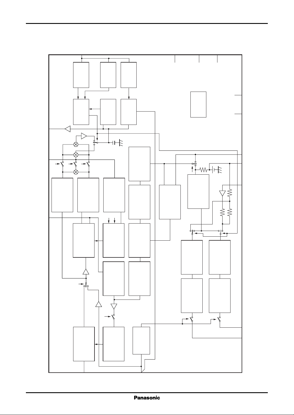
■ Block Diagram
Killer Mon.
Bell Ref.
Bell Mon.
11
7
2
Inversion
B
V
Limiter Amp.
SCP In
15
H.VBLK
generation
IH FF
B
Limiter Amp.
BGP
generation
B
generation
Reset pulse
ID discrimination
V/I conversion
B
V
VBLK
generation
V
Internal
discrimination
SECAM/Non-SECAM
V/I conversion
14
ICO
N.C.
V
N.C.
13
Band Gap
De-Emp.
12
N.C.
3
6
8
5
4
V
CC
GND
PLL Ref.
Bell Filter
Current shift
(VBLK,BGP,Signal)
B−Y Amp.
V
Limiter Amp. Phase Det. Loop Filter
Output Filter
10
9
−(B−Y) Out
−(R−Y) Out
ACC Amp.
16
C-In
B
ACC Det. Amp.
External
discrimination
SECAM/Non-SECAM
1
ref
ID/f
Output Filter R−Y Amp.
2
ICs for TV AN5637
■ Pin Descriptions
Pin No. Description
Pin No. Description
1 Reference frequency signal/
Ident input pin
2 Bell filter output monitor pin
3 Power supply pin
4 Black level adjustment voltage input pin
5 Black level adjustment reference voltage
output pin
6 Grounding pin
7 Bell filter automatic adjustment sample
hold pin
8 PLL filter automatic adjustment sample
hold pin
9 − (R−Y) output pin
10 − (B−Y) output pin
11 Killer voltage monitor pin
12 N.C.
13 N.C.
14 N.C.
15 Sand castle pulse input pin
16 SECAM signal input pin
■ Absolute Maximum Ratings
Parameter Symbol Rating Unit
Supply voltage V
Supply current I
2
Power dissipation
Operating ambient temperature
Storage temperature
Note) *1:Ta = 25 °C except operating ambient temperature and storage temperature.
*2: Power dissipation of the package at Ta = 70 °C.
*
1
*
1
*
CC
CC
P
D
T
opr
T
stg
11.0 V
73 mA
777 mW
−20 to +70 °C
−55 to +150 °C
■ Recommended Operating Range
Parameter Symbol Range Unit
Supply voltage V
CC
■ Electrical Characteristics at VCC = 9 V, Ta = 25 °C
Parameter Symbol Conditions Min Typ Max Unit
Power supply
Supply current I
Pin voltage V
Current when VCC = 9 V 304050mA
3
Voltage when VCC = 9 V 2.9 3.2 3.5 V
5
7.2 to 9.9 V
3

AN5637 ICs for TV
■ Electrical Characteristics at VCC = 9 V, Ta = 25 °C (continued)
Parameter Symbol Conditions Min Typ Max Unit
Input(Pin16) Typical input : (Pin16) Color bar signal, (Pin15) Sand castle pulse,
(Pin1) 4.43362 MHz sine wave 350 mV[p-p], V-BLK period
Input dynamic range V
1
Chroma signal input amplitude
*
V
Input impedance Z
Bell filter Typical input : (Pin16) 4.0 MHz to 4.6 MHz sine wave 10 mV[p-p],
Bell adjusting voltage V
Center frequency f
Band width B Band width of bell filter 250 3 10 370 kHz
ACC Typical input : (Pin16) Color bar signal (Composite) 1 V[p-p],
ACC characteristics 1 ACC1 Output change amount when −606%
ACC characteristics 2 ACC2 Output change amount when −606%
Demodulator/Output Typical input : (Pin16) Color bar signal (Composite) 1 V[p-p],
PLL adjusting voltage V
R−Y output amplitude V
B−Y output amplitude V
Detector output linearity L
R−Y/B−Y output ratio
2
Black level adjusting voltage
Black level error (R−Y)
Note) *1: Refer to "Explanations of testing method 1"
*2: Refer to "Explanations of testing method 2"
*
2
*
(R−Y)(B−Y)
V
f
Composite signal input amplitude 1.0 1.5 V
DR16
range
Chroma signal input amplitude range
ch.16
DC measurement 17 25 33 kΩ
16
300
(Pin15) Sand castle pulse,
(Pin1) 4.43362 MHz sine wave 350 mV[p-p], V-BLK period
Sample hold pin voltage at bell 2.8 3.9 5 V
ADB
filter automatic adjustement
Center frequency of bell filter 4.202 4.262 4.322 MHz
OB
(Signal period)
(Signal period)
(Pin15) Sand castle pulse,
(Pin1) 4.43362 MHz sine wave 350 mV[p-p], V-BLK period
discrimination signal changes from
150 mV[p-p] to 300 mV[p-p]
discrimination signal changes from
150 mV[p-p] to 15 mV[p-p]
(Pin15) Sand castle pulse,
(Pin1) 4.43362 MHz sine wave 350 mV[p-p], V-BLK period
Sample hold pin voltage at PLL 3.1 3.7 4.3 V
ADV
automatic adjustement
Color bar (Composite) signal input 0.85 1.00 1.15 V[p-p]
RY
(1 V[p-p])
Color bar (Composite) signal input 1.07 1.27 1.47 V[p-p]
BY
(1 V[p-p])
Color bar (Composite) signal input −606%
O
(1 V[p-p])
Amplitude ratio of VRY and V
Pin4 voltage when difference of 1.45 2.1 2.75 V
AD4
1.12 1.27 1.42 Times
BY
B−Y black level becomes 0
Value referred to input frequency 10 kHz
BER
mV[p-p]
4
 Loading...