

Panasonic AN5491K Datasheet
ICs for TV
AN5491K
Synchronous signal and deflection distortion correction processing IC
2
supporting I
■ Overview
The AN5491K is a deflection processor IC for synchronous signal processing and screen distortion correction. It synchronizes with the input signal of High-vision,
wide television, NTSC, PAL and VGA by the external
binary input signal of them so that a multimedia television
can be realized easily.
■ Features
• Supports the multiple-point horizontal frequency
(15.7 kHz to 62.7 kHz)
• Horizontal duty is controllable by external voltage.
• Built-in full functions for correction
(Horizontal and vertical: 16 items)
• Over-current detection, shut-down and hold-down
C bus for HD, wide television
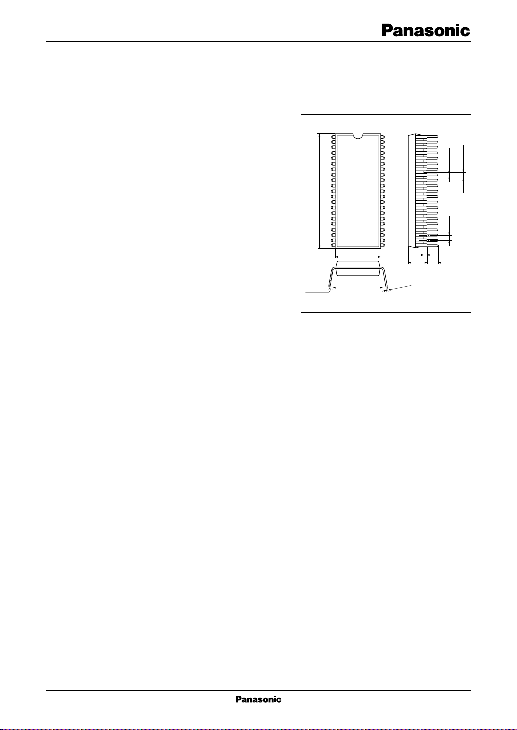
36.8±0.3
3° to 15°
Unit: mm
1
2
3
4
5
6
7
8
9
10
11
12
13
14
15
16
17
18
19
20
21
13.7±0.3
15.3±0.25
42
41
40
39
38
37
36
35
34
33
32
31
30
29
28
27
26
25
24
23
22
4.76±0.25
0.1
+
–0.05
0.3
0.5±0.1
1.778
0.96±0.25
3.3±0.25
0.9±0.25
SDIP042-P-0600A
■ Applications
• High-vision televisions, Wide screen televisions and
Projection televisions
1
AN5491K ICs for T V
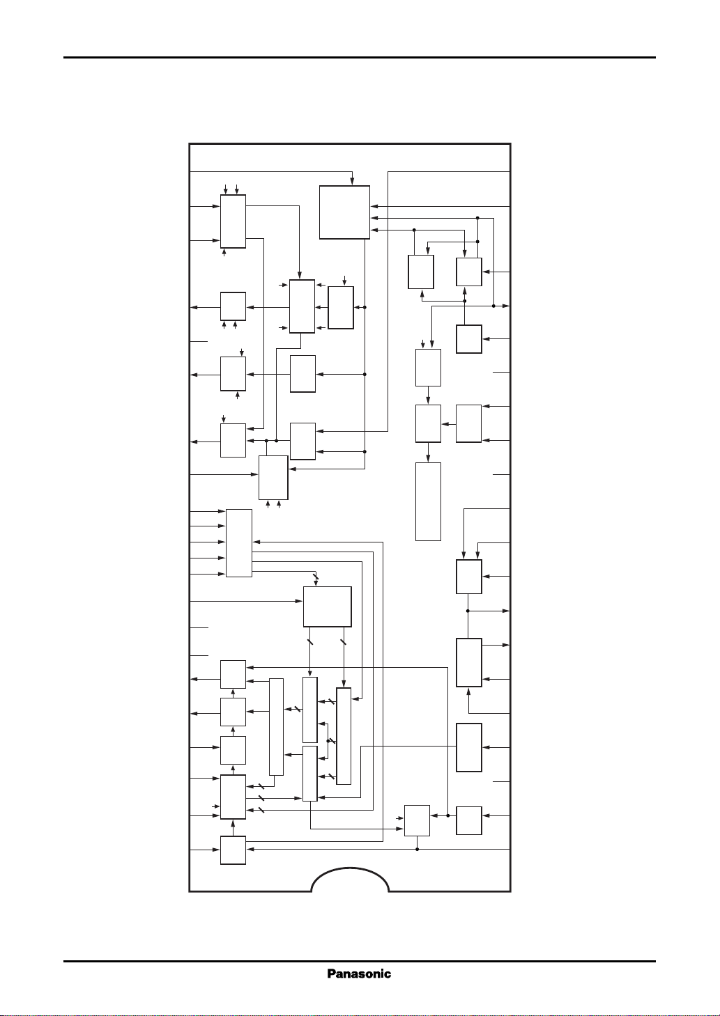
■ Block Diagram
22 21
AGC
EHT-DC
EHT-AC
V- EHT
H- EHT
23 20
/AGC
24
EHT
correction
Ramp
Trapezoid
Ramp
V-out
DEF GND
Phase out
EW out
Corner level
× 32
× 8
× 4
× 2
× 1
VGA
2
L GND
I
H-GND
Lock det.
H-out
V
VP
18
OSC
17
16
slice
15
28
29
30
EHT-AC
V
out
POL
V-POS
out
Phase
Trape
V-SAW
correction
Phase
crrection
H-parabola
V/I
converter
V-amp.
V-S
V-LIN
BOW
timing
V-AGC
Latch-SW
pulse
V-latch
14
Parallel
32
H-WID
out
EW
crrection
Trapezoid
Data
latch
2
C
I
decode
13
33 12
Corner
19
correction
11
25
Upper
H
Lower
input
5
26
31
35
switch
f
27
34
36
37 6
38 5
Lock
H
det.
out
input
Counter
2
6
7
4
Sync. DEF DAC
gen.
V-BLK
det.
X-ray
10
V-OSC
VS2
VP in
DEF V
SCL
SDA
2
I
L V
CC
V-SAW in
V-SAW lower
9
V-SAW upper
8
BLK out
7
Comparator out
Comparator in
Comparator ref.
CC
H-duty adj.
H-AFC2
FBP in
H-OSC
39 4
H
duty
Counter BF
40
H
H-POS
H
AFC2
VCO
2 2 2
41 2
42
2
Counter
7
Counter PG Counter decode
Gain-SW
H
AFC1
Shut down
HP
det.
slice
Shut down
3
H-V
H-pulse in
1
H-AFC1
CC
2
ICs for TV AN5491K
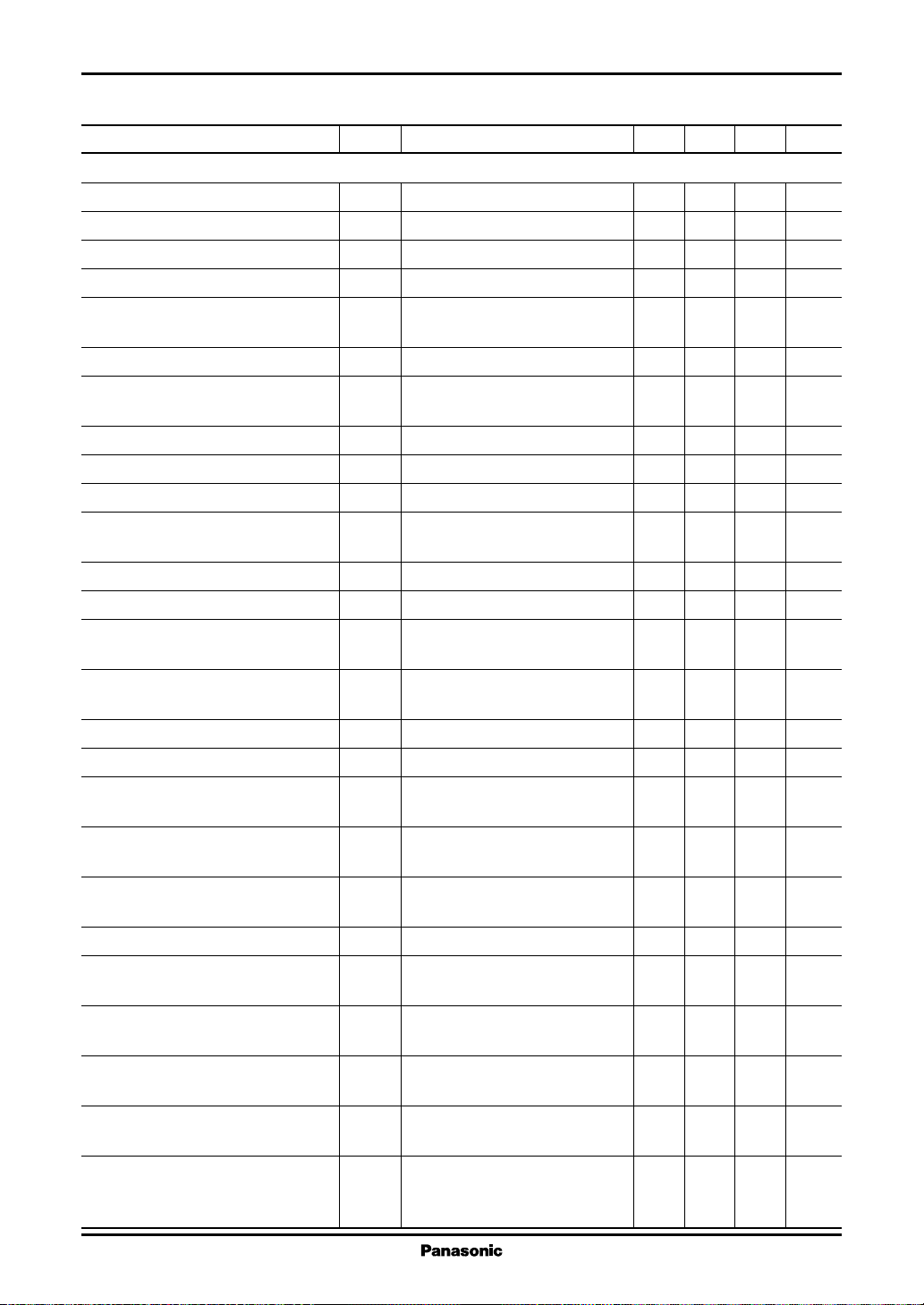
■ Pin Descriptions
Pin No. Description Pin No. Description
1 H-AFC1 22 V- AGC
2 H-pulse input 23 EHT-DC input
3H-V
4 Shut down SW 25 × 8
5 Comparator ref. (6.5 V) 26 × 4
6 Comparator 27 VGA
7 Comparator output 28 V-output
8 BLK output 29 DEF GND
9 V-SAW slice voltage (High) 30 Phase output
10 V-SAW slice voltage (Low) 31 × 2
11 V-SAW input 32 EW output
12 I2L VCC (5 V) 33 Corner slice voltage
13 I2C SDA input 34 I2L GND
14 I2C SCL input 35 × 1
15 DEF VCC (9 V) 36 H-GND
16 V-pulse input 37 Lock det.
17 V-pulse output 38 H-output
18 V-OSC 39 H-duty
19 × 32 40 H-AFC2
20 V-ramp 41 FBP input
21 Trapezoid correction voltage 42 H-OSC
(6.2 V) 24 EHT-AC input
CC
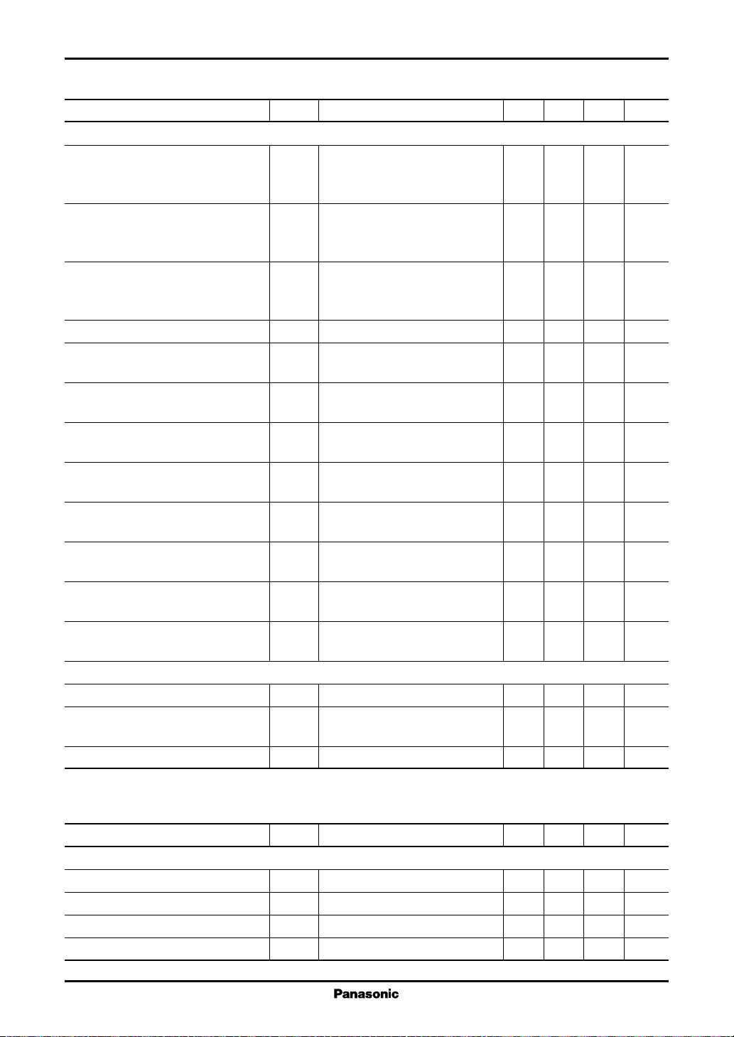
■ Absolute Maximum Ratings
Parameter Symbol Rating Unit
Supply voltage V
Supply current I
2
Power dissipation
*
Operating ambient temperature
1
Storage temperature
Note)*1: Except for the operating ambient temperature and storage temperature, all ratings are for Ta = 25°C.
2: The power dissipation shown is for the independent IC without a heat sink in free air at Ta = 70°C.
*
*
CC
CC
P
D
1
*
T
opr
T
stg
V
CC1
V
CC2
I
CC1
I
CC2
I
3
5.6 V
10
24 mA
29
14
600 mW
−20 to +70 °C
−55 to +150 °C
3
AN5491K ICs for T V
■ Recommended Operating Range
Parameter Symbol Range Unit
Supply voltage V
CC1
V
CC2
■ Electrical Characteristics at Ta = 25°C
Parameter Symbol Conditions Min Typ Max Unit
DC characteristics
Circuit current I
Circuit current I
Circuit current I
CC1
CC2
CC3
Synchronizing signal processing
Horizontal free-running oscillation f
frequency 1 [Divide-by-8] Pins 19, 26, 31, 35: Low
Horizontal free-running oscillation f
frequency 2 [Divide-by-16] Pins 19, 25, 26, 31, 35: Low
Horizontal free-running oscillation f
frequency 3 [Divide-by-32] Pin 19: High
Horizontal output pulse duty cycle 1 τ
[Divide-by-32] Pin 19: High
Horizontal output pulse duty cycle 2 τ
[Divide-by-32] Pin 19: High
Horizontal high-level output voltage V
Horizontal low-level output voltage V
Horizontal output start voltage V
Screen center variable range 1 t
[Divide-by-16] Pins 19, 26, 31, 35: High
Screen center variable range 2 t
[Divide-by-32] Change amount of phase difference
Horizontal input pulse threshold voltage
Over-voltage protective operation V
voltage
I
V
12
I
15
I
3
HO8
HO16
HO32
HO1
HO2
FHH
FHL
FHS
= 5 V, V
CC1
V
= 5 V, V
CC1
V
= 5 V, V
CC1
V
= 6.5 V
CC3
Pin 2: Without input, Pin 25: High 61.5 62.7 63.9 kHz
Pin 2: Without input 30.8 31.4 32.0 kHz
Pin 2: Without input 15.4 15.7 16.0 kHz
Pin 2: Without input, Pin 39: 2 V 11.7 14.0 16.6 µs
Pin 2: Without input, Pin 39: 5 V 23.9 28.5 33.7 µs
DC voltage for pin 38 high-level 2.8 3.5 4.2 V
DC voltage for pin 38 low-level 0 0.3 V
Minimum voltage of pin 3 to bec- 4.2 5.0 V
ome f > 10 kHz when horizontal
oscillation output is 1 V[p-p] or
more in divide-by-32 mode.
Pin 25: Low, 2.16 2.70 3.24 µs
DH16
Change amount of phase difference
between H
[00] to [1F]
Pin 19: Low, 3.8 4.8 5.8 µs
DH32
between HP and H out of Data 08:
[00] to [1F]
V
Slice level of pin 2 0.9 1.5 2.1 V
T2
Pin 4 voltage at I4 = 50 µA 0.60 0.75 0.90 V
4
4.5 to 5.0 to 5.5 V
8.1 to 9.0 to 9.9
= 9 V 13.6 17.0 20.4 mA
CC2
= 9 V 16.8 21.0 25.2 mA
CC2
= 9 V, 6.0 7.5 9.0 mA
CC2
and H-out of Data 08:
P
4
ICs for TV AN5491K
■ Electrical Characteristics at Ta = 25°C (continued)
Parameter Symbol Conditions Min Typ Max Unit
Deflection correction processing
VP pulse for OSD low-level V
VP pulse for OSD high-level V
EHT-AC input pin voltage V
Vertical input signal threshold voltage V
Vertical free-running oscillation f
LOSDVCC1
HOSDVCC1
24
TFV
VO
frequency external R = 10 kΩ, C = 3.3 µF
Typical vertical output amplitude V
Typical EW output amplitude V
Phase out amplitude V
Ramp waveform amplitude V
AGC input and output current I
Service SW: ON time V
V
EW
PHASE
RAMPfV
AGC
28SW
Vertical output DC
BLK pulse high-level V
BLK pulse low-level V
Vertical output amplitude
∆V
HBLK
LBLK
AMPmax
variable ratio (max.) typ. → max.
Vertical output amplitude
∆V
AMPmin
variable ratio (min.) typ. → max.
Vertical output DC variable amount (min.)
Vertical output DC variable amount (max.)
Vertical output trapezoidal waveform
∆V
∆V
∆V
SHIFTmin
SHIFTmax
TRAPmin
correction variable amount (min.) Typ. → min.
Vertical output trapezoidal waveform
∆V
TRAPmin
correction variable amount (max.) Typ. → max.
External trapezoidal waveform V
21
center voltage
Vertical output center DC level V
EW output (min.) to parabolic V
28
EWmin
amplitude change
EW output (max.) to parabolic V
EWmax
amplitude change
EW output (min.) (DC) ∆V
EWmin
to horizontal amplitude change
EW output (max.) (DC) ∆V
EWmax
to horizontal amplitude change
EW output (bottom voltage) 1 ∆V
EDC1
to EHT-DC change Horizontal EHT: Max.
= 5 V, V
= 5 V, V
= 9 V 0 0.4 V
CC2
= 9 V 2.2 2.75 3.3 V
CC2
Pin 24: Open 2.00 2.45 2.90 V
Pin 16: Input 0.9 1.5 2.1 V
Pin 16: Without input 35 44 53 Hz
V amplitude DAC: Typ. 0.88 1.10 1.32 V[p-p]
EW output amplitude for typical ver- 0.8 1.0 1.2 V[p-p]
tical output amplitude = 1.25 V[p-p]
Side pin parallel, DAC: Typ. − 0.1 0 0.1 V[p-p]
= 50 Hz to 120 Hz 2.15 2.45 2.75 V[p-p]
1.6 2.0 2.4 mA
3.1 3.5 3.9 V
4.5 5.0 5.5 V
0 0.4 V
V amplitude ratio between +40 +50 +60 %
V amplitude ratio between −40 −50 −60 %
Vertical DC: Typ. → min. − 0.28 − 0.38 − 0.48 V
Vertical DC: Typ. → max. +0.28 +0.38 +0.48 V
Trapezoidal waveform correction: − 0.28 − 0.38 − 0.48 V
Trapezoidal waveform correction: +0.28 +0.38 +0.48 V
2.4 3.0 3.6 V
2.8 3.5 4.2 V
Parabolic amplitude: Min. − 0.1 0 0.1 V[p-p]
Parabolic amplitude: Max. 1.4 1.8 2.2 V[p-p]
Horizontal amplitude: Min. − 0.95 −1.15 −1.35 V
Horizontal amplitude: Max. +0.95 +1.15 +1.35 V
EHT-DC: 5.0 V → 3.8 V +1.04 +1.30 +1.56 V
EHT-AC gain: Min.
5
AN5491K ICs for T V
■ Electrical Characteristics at Ta = 25°C (continued)
Parameter Symbol Conditions Min Typ Max Unit
Deflection correction processing (continued)
EW output (bottom voltage) 2 ∆V
to EHT-DC change Horizontal EHT: Max.
EW output (bottom voltage) 1 ∆V
to EHT-AC change Horizontal EHT: Max.
EW output (bottom voltage) 2 ∆V
to EHT-AC change Horizontal EHT: Max.
EW output parabolic DC level V
Parallelogram correction fluctuation 1 ∆V
(upper side) Typ. → min.
Parallelogram correction fluctuation 2 ∆V
(upper side) Typ. → max.
Parallelogram correction fluctuation 3 ∆V
(lower side) Typ. → min.
Parallelogram correction fluctuation 4 ∆V
(lower side) Typ. → max.
Bow shape correction fluctuation 1 ∆V
(upper side) Typ. → min.
Bow shape correction fluctuation 2 ∆V
(upper side) Typ. → max.
Bow shape correction fluctuation 3 ∆V
(lower side) Typ. → min.
Bow shape correction fluctuation 4 ∆V
(lower side) Typ. → max.
I2C interface
SCL, SDA input threshold voltage V
Sink capacity at ACK V
Maximum clock frequency f
EHT-DC: 5.0 V → 6.2 V −1.04 −1.30 −1.56 V
EDC2
EHT-AC gain: Min.
EHT-AC: 2.35 V → 1.35 V +0.25 +0.35 +0.45 V
EAC1
EHT-AC gain: Max.
EHT-AC: 2.35 V → 3.35 V − 0.25 − 0.35 − 0.45 V
EAC2
EHT-AC gain: Max.
Typ. 2.2 2.7 3.4 V
32
Parallelogram correction: +0.16 +0.26 +0.36 V
UPH1
Parallelogram correction: − 0.16 − 0.26 − 0.36 V
UPH2
Parallelogram correction: − 0.25 − 0.35 − 0.45 V
BPH1
Parallelogram correction: +0.16 +0.26 +0.36 V
BPH2
Bow shape correction: − 0.24 − 0.34 − 0.44 V
USD1
Bow shape correction: +0.12 +0.22 +0.32 V
USD2
Bow shape correction: − 0.17 − 0.27 − 0.37 V
BSD1
Bow shape correction: +0.12 +0.22 +0.32 V
BSD2
V
TH
ACK
= 5 V 1.5 3.0 dB
CC1
I = 3 mA in case of pull-up resistor 0.4 V
1.6 Ω
SCL
100 kHz
• Design reference data
Note) The characteristics listed below are theoretical values based on the IC design and are not guaranteed.
Parameter Symbol Conditions Min Typ Max Unit
DC characteristics
AGC pulse width τ
Ramp discharge current I
Ramp charge current 1 I
Ramp charge current 2 I
AGC
RAMP1
RAMP2
RAMP3
f = 120 Hz, Pin 4: 5.7 V 138 µA
f = 30 Hz, Pin 4: 7.5 V 32.9 µA
95 µs
3.6 mA
6
 Loading...