

Panasonic AN5452 Datasheet
ICs for TV
AN5452
IC for landing correction
■ Overview
The AN5452 is an IC to drive a landing correction coil
of CRT monitor. The circuit is suitable for low power
consumption design.
■ Features
• Built-in power amplifier (±200 mA)
• Low standby current (typ.: 2 mA)
• Incorporating 2 circuits
■ Applications
• CRT monitors
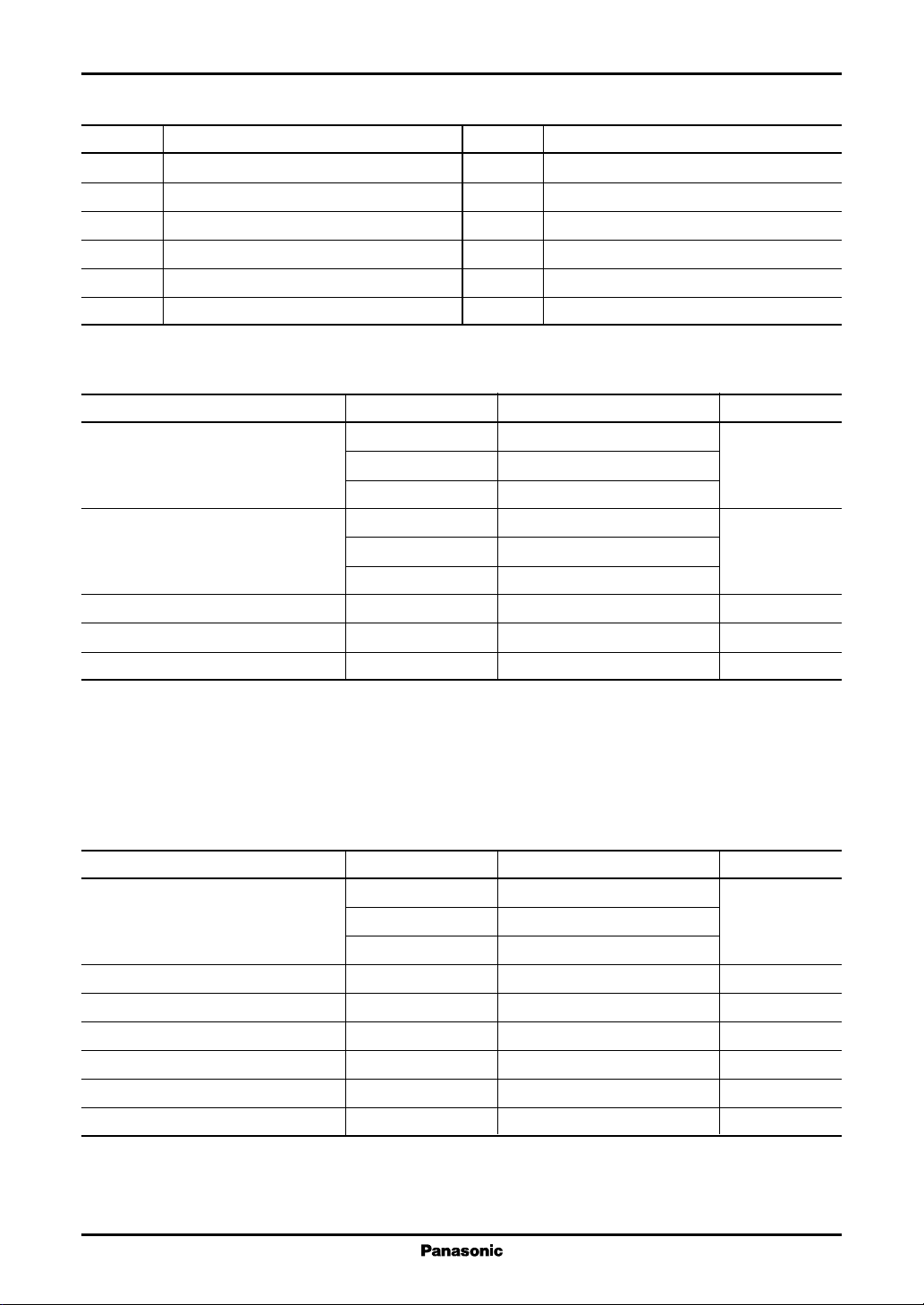
■ Block Diagram
CC1
V
1
CC3VCC2
V
3
2
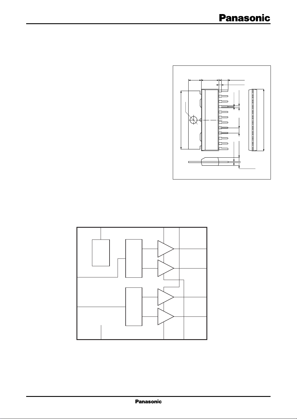
28.0±0.3
5.8±0.25
φ3.3
7.9±0.3
HSIP012-P-0000
3.5±0.25
1.2±0.25
12
11
10
9
8
7
6
5
4
3
2
+0.1
1
0.5±0.1
−0.05
0.45
Unit: mm
1.2±0.25
2.54
1.7±0.25
1.7±0.25
29.4±0.3
+
7
Bias
Control-1
−
8
4
+
10
5
11
6
GND3
12
GND1
Control-2
−
9
GND2
1
AN5452 ICs for TV
■ Pin Descriptions
Pin No. Description
1 Control block power supply 12 V (V
2 Output block power supply 12 V (V
3 Output block power supply 12 V (V
CC2
CC3
4 Landing1 control input
5 Landing2 control input
6 Output block GND (GND3)
■ Absolute Maximum Ratings
Parameter Symbol Rating Unit
Supply voltage V
Supply current I
Power dissipation
Operating ambient temperature
Storage temperature
Note)
1: Except for the power dissipation, operating ambient temperature, and storage temperature, all ratings are for Ta = 25°C.
1. *
2: The power dissipation for the independent package (without a heat sink) at Ta = 75°C. Refer to "■ Technical Informa-
*
tion" for details.
Be sure to comply with "■ Usage Notes" for the sequence of turning on power supply.
3.
Refer to "■ Usage Notes" in case of using the IC at V
4.
*2
*1
*1
CC1
V
CC2
V
CC3
CC1
I
CC2
I
CC3
P
D
T
opr
T
stg
Pin No. Description
CC1
)
)
)
7 Landing1 positive output
8 Landing2 negative output
9 Output block GND (GND2)
10 Landing2 positive output
11 Landing2 negative output
12 Control block GND (GND1)
13.5 V
13.5
13.5
35 mA
200
200
1 171 mW
−20 to +75 °C
−55 to +150 °C
, V
CC3
≤ 8 V
CC2
■ Recommended Operating Range
Parameter Symbol Range Unit
Supply voltage V
Landing1 control input V
Landing2 control input V
Landing1 positive output I
Landing1 negative output I
Landing2 positive output I
Landing2 negative output I
2
CC1
V
CC2
V
CC3
4-12
5-12
7
8
10
11
10.8 to 13.2 V
7.0 to 13.2
7.0 to 13.2
0 to 6 V
0 to 6 V
−200 to +200 mA
−200 to +200 mA
−200 to +200 mA
−200 to +200 mA
ICs for TV AN5452
■ Recommended Operating Range (continued)
Parameter Symbol Range Unit
Peak current I
Note)
The peak current characteristic is the reference value for design. The shipping inspection of it is not performed.
For the evaluating conditions, refer to "■ Electrical Characteristics • Explanations of testing method".
I
I
I
7(P)
8(P)
10(P)
11(P)
■ Electrical Characteristics at Ta = 25°C
Parameter Symbol Conditions Min Typ Max Unit
Circuit current 1 I
Circuit current 2 I
Circuit current 3 I
Circuit voltage 7 V
Circuit voltage 8 V
Circuit voltage 10 V
Circuit voltage 11 V
Landing1 output voltage 1 E
Landing1 output voltage 2 E
Landing1 output voltage 3 E
Landing2 output voltage 1 E
Landing2 output voltage 2 E
Landing2 output voltage 3 E
V
CC1
CC2
CC3
10−9VCC1
11−9VCC1
1(1)V7-V8
1(2)V7-V8
1(3)V7-V8
2(1)V10-V11
2(2)V10-V11
2(3)V10-V11
CC1
V
CC1
V
CC1
7−6VCC1
8−6VCC1
= 12 V, V
= 12 V, V
= 12 V, V
= 12 V, V
= 12 V, V
= 12 V, V
= 12 V, V
CC2
CC2
CC2
CC2
CC2
CC2
CC2
= V
= V
= V
= V
= V
= V
= V
at V4 = 2.5 V − 0.3 0.0 +0.3 V
at V4 = 5 V +5.1 +5.5 +5.9 V
at V4 = 0 V −5.9 −5.5 −5.1 V
at V5 = 2.5 V − 0.3 0.0 +0.3 V
at V5 = 5 V +5.1 +5.5 +5.9 V
at V5 = 0 V −5.9 −5.5 −5.1 V
−0.7 to +0.7 A
−0.7 to +0.7
−0.7 to +0.7
−0.7 to +0.7
= 12 V 1.5 3.0 4.5 mA
CC3
= 12 V 01mA
CC3
= 12 V 01mA
CC3
= 12 V 4.1 4.5 4.9 V
CC3
= 12 V 4.1 4.5 4.9 V
CC3
= 12 V 4.1 4.5 4.9 V
CC3
= 12 V 4.1 4.5 4.9 V
CC3
• Design reference data
Note) The characteristics listed below are theoretical values based on the IC design and are not guaranteed.
Parameter Symbol Conditions Min Typ Max Unit
Landing1 output fluctuation ∆E
with high-level supply voltage V
Landing1 output fluctuation ∆E
with low-level supply voltage V
Landing2 output fluctuation ∆E
with high-level supply voltage V
Landing2 output fluctuation ∆E
with low-level supply voltage V
Landing1 output fluctuation with ∆E
/V
1
CCH
/V
1
CCI
/V
2
CCH
/V
2
CCI
1 /Ta
= 12 V → 13.2 V, − 0.2 +0.2 V
CC1
∆E at V
CC1
∆E at V
CC1
∆E at V
CC1
∆E at V
= 12 V → 13.2 V
CC2, 3
= 12 V → 10.8 V, − 0.2 +0.2 V
= 12 V → 10 V
CC2,3
= 12 V → 13.2 V, − 0.2 +0.2 V
= 12 V → 13.2 V
CC2,3
= 12 V → 10.8 V, − 0.2 +0.2 V
= 12 V → 10 V
CC2,3
∆E at Ta = +25°C → −25°C and − 0.2 +0.2 V
temperature Ta = +25°C → +70°C
Landing2 output fluctuation with ∆E
∆E at Ta = +25°C → −25°C and − 0.2 +0.2 V
2 /Ta
temperature Ta = +25°C → +70°C
3
 Loading...