

Panasonic AN5448 Datasheet
ICs for TV
AN5448
TILT correction IC
■ Overview
The AN5448 is a rotation (TILT) correction IC in
which the control circuit and the drive circuit are integrated on a single chip.
■ Features
• TILT output range: 1.7 V to 7.4 V
• Maximum output current: 200 mA
• Frequency characteristics: 200 kHz
■ Applications
• CRT monitor
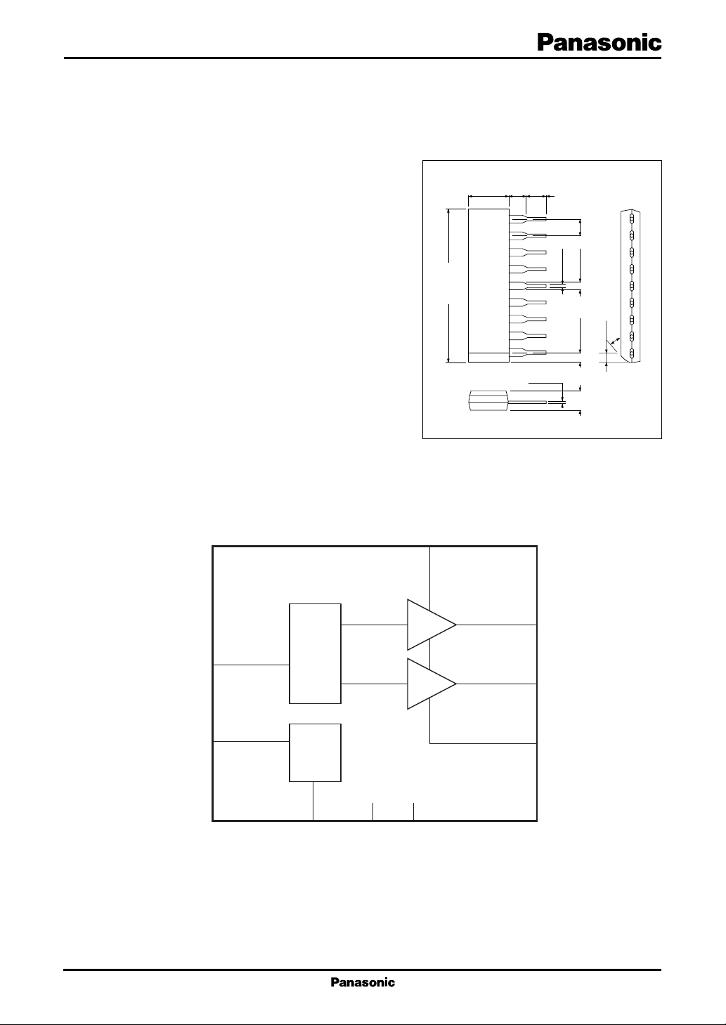
■ Block Diagram
0.5±0.1
2.54
1.5±0.25
1.5±0.25
3.0±0.3
Unit: mm
30°
1.4±0.3
CC2
V
23.3±0.3
6.0±0.3
2.4±0.25
3.3±0.25
9
8
7
6
5
4
3
2
1
+0.1
0.3
−0.05
SIP009-P-0000C
2
+
4
In
−
1
V
CC1
Bias
9
GND1
3
N.C.
6
N.C.
7
8
5
GND2
1
AN5448 ICs for TV
■ Pin Descriptions
Pin No. Description
1 Supply voltage 12 V (V
2 Output block supply voltage 12 V (V
3N.C.
4 TILT control input
5 Output block GND (GND2)
6N.C.
7 TILT positive output
8 TILT negative output
9 GND (GND1)
■ Absolute Maximum Ratings
Parameter Symbol Rating Unit
Supply voltage V
Supply current I
2
Power dissipation
Operating ambient temperature
Storage temperature
Note) Be sure to comply with "■ Usage Notes" for the sequence of turning on power supply.
1: Except for the power dissipation, operating ambient temperature and storage temperature, all ratings are for Ta = 25°C.
*
2: The power dissipation shown is for the IC package at Ta = 75°C. Refer to "■ Technical Information" for details.
*
*
1
*
1
*
CC1
CC
CC
)
)
CC2
V
CC1
V
CC2
I
CC1
I
CC2
P
D
T
opr
T
stg
13.5 V
13.5
30 mA
200
524 mW
−20 to +75 °C
−55 to +150 °C
■ Recommended Operating Range
Parameter Symbol Range Unit
Supply voltage V
TILT control input V
TILT positive output I
TILT negative output I
Peak current I
Note) For the conditions in evaluating the peak current, refer to "■ Electrical Characteristics • Explanations of testing method".
CC1
V
CC2
4-9
7
8
7
I
8
2
10.8 to 13.2 V
7.4 to 13.2
0 to 6 V
−200 to +200 mA
−200 to +200 mA
− 0.3 to +0.3 A
− 0.3 to +0.3

ICs for TV AN5448
■ Electrical Characteristics at Ta = 25°C
Parameter Symbol Conditions Min Typ Max Unit
Circuit current (pin 1) I
Circuit current (pin 2) I
Circuit voltage (pin 7) V
Circuit voltage (pin 8) V
Output voltage difference (1) V
Output voltage difference (2) V
Output voltage difference (3) V
7-8 (1)
7-8 (2)
7-8 (3)
• Design reference data
Note) The characteristics listed below are theoretical values based on the IC design and are not guaranteed.
Parameter Symbol Conditions Min Typ Max Unit
TILT output fluctuation
∆V
with supply voltage (high) V
TILT output fluctuation
∆V
with supply voltage (low) V
TILT output fluctuation ∆V
with temperature T
V
CC1
CC2
7-5
8-5
CC1
V
CC1
V
CC1
V
CC1
= 12 V, V
= 12 V, V
= 12 V, V
= 12 V, V
= 12 V 0.6 1.8 4.0 mA
CC2
= 12 V 01mA
CC2
= 12 V 4.1 4.5 4.9 V
CC2
= 12 V 4.1 4.5 4.9 V
CC2
V7 −V8 at V4 = 2.5 V − 0.45 0 +0.45 V
V7 −V8 at V4 = 5 V 5.3 5.7 6.1 V
V7 −V8 at V4 = 0 V −6.1 −5.7 −5.3 V
V
7-8
V
CCH
V
7-8
V
CC1
7-8/TaVIN
= 12 V → 13.2 V, ∆V
CC1
= 12 V → 13.2 V
CC2
= 12 V → 10.8 V, ∆V
CC1
= 12 V → 10.8 V
CC2
= 2.5 V, ∆V
= +25°C → +75°C and
a
at ±0.2 V
7-8
at ±0.2 V
7-8
at ±0.2 V
7-8
Ta = +25°C → −20°C
• Explanations of testing method
Conditions on evaluation of the peak current
1
2
3
4
5
6
7
8
9
V
CC
12 V
20 µF
CC1VCC2
V
24 Ω
N.C.
GND2
22 Ω/10 W
N.C.
12 V
300
A
mA
GND1
CloseOpen
6.8 kΩ
5 kB
1 s 1 s
Confirm that the IC operates normally after turning on and off SW 100 times at the interval of one second.
Carry out the above test when pin 7 is replaced with pin 8.
3
 Loading...