

Panasonic AN5441S Datasheet
ICs for TV
AN5441S
Deflection distortion correction IC
■ Overview
The AN5441S is a distortion correction processing IC
for deflection system of color televisions and wide screen
televisions.
■ Features
• Distortion correcting functions
• Vertical amplitude
• Vertical linearity
• Vertical S-shape
• Vertical position
• Vertical EHT
• Horizontal amplitude
• EW parabola
• Trapezoidal
• Upper/lower EW corner
• Horizontal EHT
• Built-in horizontal and vertical blanking pulse genera-
tion circuit
• Supports I
2
C bus control
■ Applications
• Color televisions and wide screen televisions
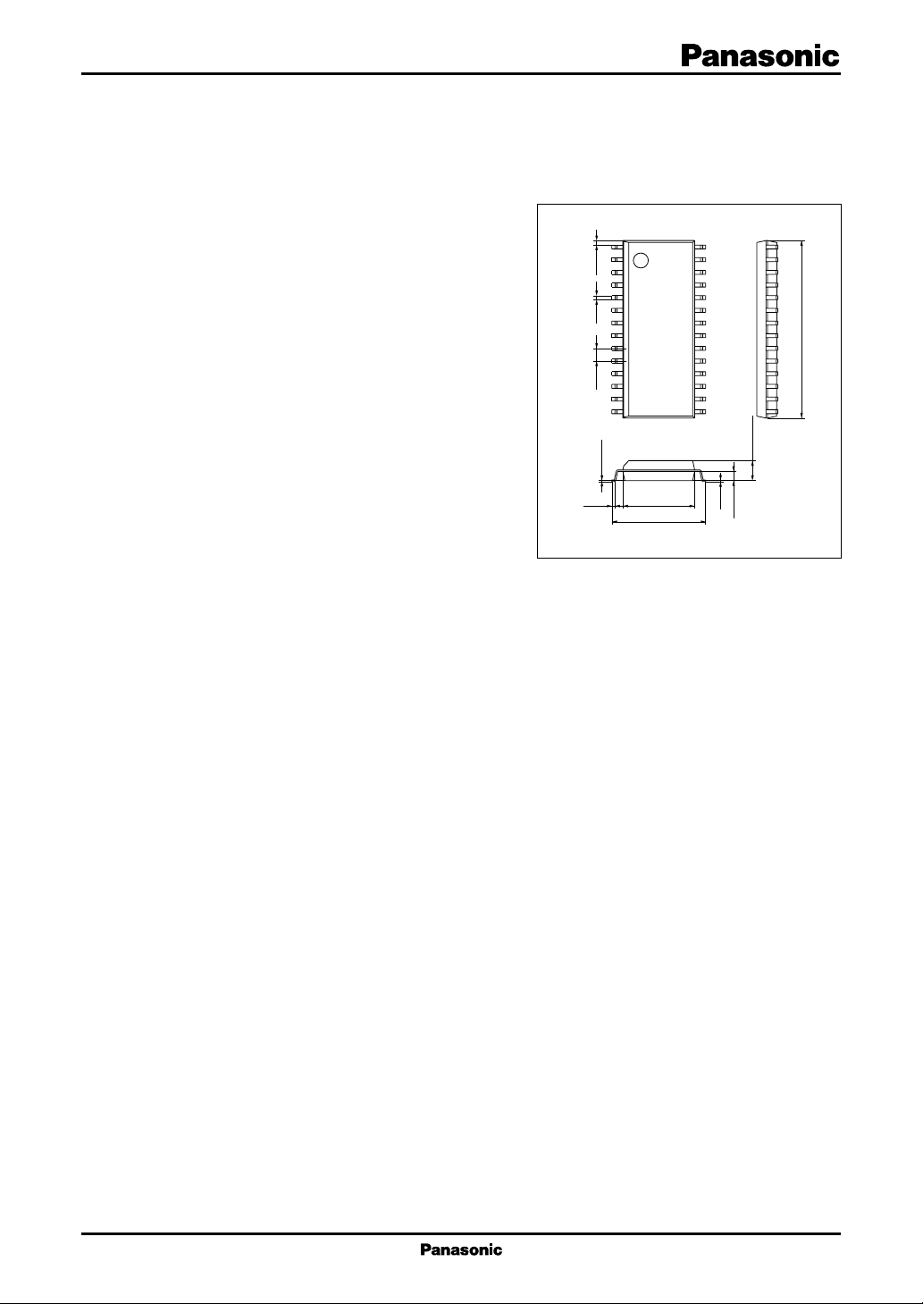
1
0.45
0.4±0.25
1.27
14
0.1±0.1
0.3
28
15
7.2±0.3
9.4±0.3
SOP028-P-0375A
0.15
Unit: mm
17.81±0.3
2.0±0.2
0.925
1
AN5441S ICs for T V
■ Block Diagram
N.C.
Corner slice
6
5
19
EW out
18
control
H-amplitude
correction
EW corner
control
V-amplitude
S-shaped
Linearity
correction
V/I
conversion
correction
Superimposed
V out
17
16
caption control
External
trapezoidal
Feedback
correction
EHT correction
2
20
Gain control
21
C
I
22
15
EHT (AC)
EHT (DC)
1
SDA
2
SCL
4
V
Key (DC)
V
CC1
CC3
(5 V)
(12 V)
23
13
Ramp
Broken neck
generation
12
24
VAGC
GND2
GND1
25
27
28
Pulse
shaping
26
VD
3
FBP
H-BLK
generation
7
HAGC
8
11
V-BLK
generation
9
10
14
V
(12 V)
CC2
Horizontal
and vertical
BLK output
V-SAW
2
ICs for TV AN5441S
■ Pin Descriptions
Pin No. Description
1I
2I
2
C SDA input
2
C SCL input
3 Horizontal FBP input
4V
CC1
(5 V)
5 Test pin
6N.C.
7 H-BLK high-level slice voltage
8 H-BLK low-level slice voltage
9 V-BLK high-level slice voltage
10 V-BLK low-level slice voltage
11 Capacitor for H-AGC
12 Horizontal and vertical BLK output
13 Broken neck detection
14 V-BLK sawtooth input
Pin No. Description
15 V
CC3
(12 V)
16 Vertical feedback input
17 Vertical pre-drive output
18 EW output
19 Corner slice voltage
20 EHT-AC input
21 EHT-DC input
22 Control for keystone correction
23 Capacitor for ramp generation
24 Capacitor for V-AGC
25 V
CC2
(12 V)
26 VD pulse input
27 GND2
28 GND1
■ Absolute Maximum Ratings
Parameter Symbol Rating Unit
Supply voltage V
Supply current I
Power dissipation
Operating ambient temperature
Storage temperature
Note)*1 : Except for the operating ambient temperature and storage temperature, all ratings are for Ta = 25°C.
2 : The power dissipation shown is the value for Ta = 70°C.
*
*2
*2
*1
CC
CC
V
CC1
V
, V
CC2
CC3
I
CC1
I
CC2
I
CC3
P
D
T
opr
T
stg
5.6 V
13.4
24.5 mA
24.0
3.2
449 mW
−20 to +70 °C
−55 to +150 °C
■ Recommended Operating Range
Parameter Symbol Range Unit
Supply voltage V
CC1
V
CC2
V
CC3
4.5 to 5.5 V
10.8 to 13.2
10.8 to 13.2
3
AN5441S ICs for T V
■ Electrical Characteristics at Ta = 25°C
Parameter Symbol Conditions Min Typ Max Unit
Circuit current I
Circuit current I
Circuit current I
CC1
CC2
CC3
EHT-AC input pin voltage V
Vertical pull-in frequency 1 f
Vertical pull-in frequency 2 f
Typical vertical output amplitude e
Typical EW output amplitude e
Vertical BLK output pulse width t
Horizontal BLK output pulse width 1
Horizontal BLK output pulse width 2
Vertical output amplitude change
ratio (max.) e
Vertical output amplitude change
ratio (min.) e
Vertical output S-shape change ratio 1
Vertical output S-shape change ratio 2
Vertical output (upper side) ∆e
linearity change ratio 1 max.
Vertical output (upper side) ∆e
linearity change ratio 2 max.
Vertical output position change ∆e
amount (max.)
Vertical output position change ∆e
amount (min.)
Vertical output (lower side) Vertical linearity (lower side) typ. → 81216%
linearity change ratio 1 max.
Vertical output (lower side) Vertical linearity (lower side) typ. →−16 −12 − 8%
linearity change ratio 2 min.
Vertical output EHT-DC change ∆e
Vertical output EHT-AC change 1 ∆e
Vertical output EHT-AC change 2 ∆e
Vertical output superimposed ∆e
caption change 1 max.
Vertical output superimposed ∆e
caption change 2 max., V amplitude typ. → min.
I
V
4
I
V
25
I
V
15
20-27, 28VCC1
V1fV
V2fV
typ. 2.3 2.7 3.1 V[p-p]
V(typ)
typ. 1.42 1.82 2.22 V[p-p]
E(typ)
Wide 3.3 4.8 6.2 ms
VB
t
t
e
e
∆e
∆e
Normal 11.7 12.2 12.7 µs
HB(1)
Wide 37 39 41 µs
HB(2)
V amplitude typ. → max. ratio 42 48 54 %
v(max)
v(typ)
V amplitude typ. → min. ratio −54 −48 − 42 %
v(min)
v(typ)
Vertical S-shape min. → max. ratio −20 −13 −6%
VS1
Vertical S-shape min. → max. ratio 1.5 6.0 %
VS2
(change of V out 40% to 60% point)
Vertical linearity (upper side) typ. → 61014%
VC1
Vertical linearity (upper side) typ. →−14 −10 −6%
VC2
Vertical position typ. → max. −1.0 − 0.8 − 0.6 V
VP(max)
Vertical position typ. → min. 0.5 0.7 0.9 V
VP(min)
EHT-DC = 6 V, −24.8 −21.8 −18.8 %
VED
vertical EHT, min. → max.
EHT-AC = 2V, VEHT: max., −16 −12 −8%
VEA(1)
EHT gain, min. → max.
EHT-AC = 4 V, VEHT: max., 9 13 17 %
VEA(2)
EHT gain, min. → max.
Vertical superimposed caption min. →−13 −10 −7%
VJ(1)
Vertical superimposed caption min. →−15 −11 −7%
VJ(2)
= 5 V, V
CC1
= 5 V, V
CC1
= 5 V, V
CC1
= 5 V, V
= 12 V, V
CC2
= 12 V, V
CC2
= 12 V, V
CC2
= 12 V, V
CC2
= 12 V 11.7 17.0 20.2 mA
CC3
= 12 V 13.1 16.6 20.2 mA
CC3
= 12 V 1.8 2.1 2.3 mA
CC3
= 12 V 2.6 3.0 3.4 V
CC3
= 50 Hz input 45 50 55 Hz
= 60 Hz input 55 60 65 Hz
4
 Loading...