

Panasonic AN5394FB Datasheet
ICs for TV
AN5394FB
RGB processor IC for the HDTV (Japan) and wide-screen TV
■ Overview
The AN5394FB is an RGB processor IC which converts the brightness and color difference signals to a primary color signal. It can be connected to each input signal of HDTV (Japan), DVD, NTSC, PAL, VGA, etc. and
facilitates rationalization and high performance of the endproducts.
■ Features
• Wider band for signal processing (Y: 30 MHz/−3 dB,
color difference: 15 MHz/−3 dB)
• Direct input of HD, NTSC and DVD standard YUV signal
• High picture quality due to the built-in various correction circuits of Y signal
• Auto-cut off functions
• Having 2 systems of RGB input, OSD plus character
broadcasting or external RGB input such as VGA is
supported.
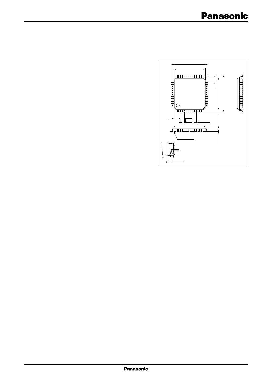
• SMD package allows for high density mounting.
■ Applications
• HDTV (Japan), wide-screen television, projection television, plasma display panel (PDP), LCD projector,
video capture board
0.15
−0.05
37
48
(1.60)
(1.00)
+0.10
14.00±0.30
12.00±0.20
36 25
0.80
Seating plane
°
0° to 10
0.50±0.20
QFP048-P-1212B
0.30
Unit: mm
(1.60)
24
14.00±0.30
12.00±0.20
13
121
+0.10
−0.05
0.10±0.10 1.95±0.20
1
AN5394FB ICs for TV
■ Block Diagram
Y in
R-Y in
B-Y in
Chroma γ cont.
ABL/ACL
Analog GND1
CLP in
5 V
V
CC
DI in
BLK in
HP in
VP in
37
38
39
40
41
42
43
44
45
46
47
48
R-Y
B-Y
White peak det.
Black peak det.
36
35
34
Y
Video
block
Chroma
block
ABL/ACL
block
I2C block
Pulse block
APL det.
R-CLP
33
R-Y
G-Y
B-Y
G-CLP
32
Matrix
block
B-CLP
31
9 V
CC
Analog V
30
RY'
G
B
RGB
CC2
Spot killer in
RGB out-V
29
28
RGB out
block
RGB (OSD)
OSD block
CC1
RGB out-V
Blooming DC in
27
26
25
IK
24
R-S/H
23
R-out
22
G-S/H
21
G-out
20
B-S/H
19
B-out
18
RGB out-GND1
17
RGB out-GND2
16
Analog V
15
OSD-R in
14
OSD-G in
13
OSD-B in
CC2
1
2
3
4
5
6
7
8
9
10
11
12
Ys
VP+6H
YM
RGB SW
SCL
NECK in
SDA
R-in
G-in
B-in
GND 5 V
Analog GND2
2
ICs for TV AN5394FB
■ Pin Descriptions
Pin No. Description
1 VP + 6H
2 RGB SW
3 YM input
4 Ys input
5 Neck in
6 SCL
7SDA
8 GND 5 V
9 R-n
10 G-in
11 B-in
12 Analog GND2
13 OSD-B in
14 OSD-G in
15 OSD-R in
16 Analog V
CC2
17 RGB out-GND2
18 RGB out-GND1
19 B output
20 B-S/H
21 G output
22 G-S/H
23 R output
24 R-S/H
Pin No. Description
25 IK
26 Blooming DC in
27 RGB out-V
28 RGB out-V
CC1
CC2
29 Spot killer in
30 Analog V
CC1
31 B-CLP
32 G-CLP
33 R-CLP
34 APL det.
35 Black peak det.
36 White peak det.
37 Yin
38 R−Y in
39 B− Y in
40 Chroma γ cont.
41 ABL/ACL
42 Analog GND1
43 CLP in
44 VCC 5V
45 DI in
46 BLK in
47 HP in
48 VP in
■ Absolute Maximum Ratings
Parameter Symbol Rating Unit
Supply voltage V
Supply current I
2
Power dissipation
Operating ambient temperature
Storage temperature
Note)*1 : Except for the operating ambient temperature and storage temperature, all ratings are for Ta = 25°C.
2 : Power dissipation PD indicates the value in the free air at Ta = 70°C. For further details, refer to "■ Technical Information".
*
*
1
*
1
*
CC1
V
CC2
CC1
I
CC2
P
D
T
opr
T
stg
10.0 V
5.6
70.0 mA
39.2
681 mW
−25 to +70 °C
−55 to +150 °C
3
AN5394FB ICs for TV
■ Recommended Operating Range
Parameter Symbol Range Unit
Supply voltage V
CC1
V
CC2
8.1 to 9.9 V
4.5 to 5.5
■ Electrical Characteristics at V
= 9 V, V
CC1
= 5 V, Ta = 25°C
CC2
Parameter Symbol Conditions Min Typ Max Unit
(1) DC characteristics
Circuit current 1
*
I
CC1
V
CC1
= 9 V, V
= 5 V 395163mA
CC2
1
No signal input
1
Circuit current 2
*
I
CC2
V
CC1
= 9 V, V
= 5 V 243135mA
CC2
No signal input
(2) Y-system
Video voltage gain AY
Input: Sine wave 0.2 V[p-p] 4.4 5.4 6.4 Times
G
f = 1 MHz; Contrast: max.
Video voltage gain change ∆AY Ratio between R,G and B −2.5 0 2.5 dB
Drive: typ.
Frequency characteristics fY Input: Sine wave 0.2 V[p-p] −6 −31 dB
f = 30 MHz; Contrast: max.
Standard output pedestal DC
Brightness variable range V
Brightness: typ. 2.6 3.0 3.4 V
P
Brightness: min. → max. 1.8 2.2 2.6 V
BR
Contrast ratio A(CON) Contrast: min. → max. 25 dB
APL detection voltage V
Input: Total white 0.7 V[0-p] 0.7 0.93 1.3 V
APL
Voltage at APL detection pin 34
APL detection ratio ∆
Input: Total white 0.7 V[0-p] → 0.35 V[0-p]
APL
0.44 0.54 0.64 Times
Voltage at APL detection pin 34
DC regeneration ratio 1 DC1 Input signal APL 10% → 90% 95 100 105 %
APL detection pin 34 = 0 V
DC regeneration ratio 2 DC2 Input signal APL 10% → 90% 70 80 90 %
DC regeneration SW/on; Polarity '−'
APL det./R = 75 kΩ
DC regeneration ratio 3 DC3 Input signal APL 10% → 90% 110 120 130 %
DC regeneration SW/on; Polarity '+'
APL det./R = 75 kΩ
Output blooming level V
Input: Total white 1.4 V[0-p] 5.7 6.7 7.7 V
BL
Blooming DC
= 3.8 V
Pin 34: 0 V; Brightness: max.
Output blooming level change ∆V
Input: Total white 1.4 V[0-p] −1.2 − 0.9 − 0.7 V
BL
Blooming DC = 3.8 V → 4.2 V
Pin 34: 0 V; Brightness: max.
Note)*1: I
is a total of the current at pins 16, 27, 28 and 30. I
CC1
is a total of the current at pin 44.
CC2
4
ICs for TV AN5394FB
■ Electrical Characteristics at V
= 9 V, V
CC1
Parameter Symbol Conditions Min Typ Max Unit
(2) Y-system (continued)
2
*
White gradation correction 1
White gradation correction 2
Black extension Y
3
characteristics 1
*
Black extension Y
3
characteristics 2
*
Black extension Y
3
characteristics 3
*
Black extension Y
4
characteristics 4
*
Black extension Y
4
characteristics 5
*
Black extension Y
4
characteristics 6
*
White character correction 1
White character correction 2
White character correction off
5
ABL off
ABL start 1
ABL start 2
ABL gain 1
Note)*2: Adjust the blooming DC voltage (pin 26).
*
5
*
5
*
5
*
3: Black gradation SW: On
*
4: Black gradation SW: On, brightness: max.
*
5: ABLSW: On, brightness: max.
*
Yγ1 Input: Total white 0.7 V[0-p] 10 16 22 %
2
*
Yγ2 Input: Total white 0.7 V[0-p] −26 −20 −14 %
BL1
BL2
BL3
BL4
BL5
BL6
2
*
V
W1
2
*
V
W2
2
*
W
OFF
V
ABL1
V
ABL2
V
ABL3
A
ABL
= 5 V, Ta = 25°C (continued)
CC2
Gain: max. Level: typ. → max.
White gradation SW: On
Gain: max. Level: typ. → min.
White gradation SW: On
Output amplitude 0 V[p-p] − 0.1 0 0.1 V
Level: typ., gain: min. → max.
Input: Total white 0.7 V[0-p] − 0.86 − 0.66 − 0.46 V
Output amplitude1.0 V[0-p], contrast adj
level: typ., gain: min. → max.
Input: Total white 0.7 V[0-p] − 0.1 0 0.1 V
Output amplitude1.6 V[0-p], contrast adj
level: typ., gain: min. → max.
Black detection open → 3 V − 0.8 − 0.6 − 0.4 V
Level: typ., gain: typ.
Black detection open → 3 V −1.5 −1.1 − 0.7 V
Level: typ., gain: max.
Black detection open → 3 V −1.20 − 0.75 − 0.30 V
Level: min. → max., gain: typ.
Input: Total white 0.7 V[0-p] 10.0 25.0 40.0 %
Blooming DC adjustment
Level: max., gain: min. → typ.
Input: Total white 0.7 V[0-p] −9.3 0 9.3 %
Blooming DC adjustment
Level: min., gain: min. → max.
Y input: Total white 0.7 V[0-p] − 0.2 0 0.2 V
C-Y input: 0.2 V[0-p]
Level: min., gain: min. → max.
ABL/ACL pin 7.5 V − 0.1 0 0.1 V
Level: min., gain: min. → max.
ABL/ACL pin 3 V 0.28 0.39 0.50 V
Level: min. → max., gain: max.
ABL/ACL pin 3 V − 0.84 − 0.64 − 0.44 V
Level: min., gain: min. → max.
ABL/ACL pin 5 V → 3 V − 0.48 − 0.37 − 0.26 V
Level: typ., gain: max.
5
AN5394FB ICs for TV
■ Electrical Characteristics at V
= 9 V, V
CC1
= 5 V, Ta = 25°C (continued)
CC2
Parameter Symbol Conditions Min Typ Max Unit
(2) Y-system (continued)
ACL off
*
A
Input: Total white 0.7 V[0-p] −50 5 %
ACL1
6
ABL/ACL pin: 7.5 V
Level: min., gain: min. → max.
6
ACL start 1
*
A
Input: Total white 0.7 V[0-p] 10 20 30 %
ACL2
ABL/ACL pin: 3 V
Level: min. → max., gain: typ.
6
ACL start 2
*
A
Input: Total white 0.7 V[0-p] −45 −35 −25 %
ACL3
ABL/ACL pin: 3 V
Level: min., gain: min. → typ.
ACL gain 1
*
A
Input: Total white 0.7 V[0-p] −34 −22 −10 %
ACL4
6
ABL/ACL pin: 5 V → 3 V
Level: typ., gain: typ.
(3) Color difference-system
Color difference voltage gain
G
Input: Sine wave 0.2 V[p-p] 4.64 5.80 6.96 Times
R
f = 1 MHz, R−YIN → R
OUT
7
*
Color difference frequency fc Input: Sine wave 0.2 V[p-p] − 6 − 3 + 2dB
7
characteristics
B−Y axis gain adjustment range G
NTSC1
*
7
*
f = 10 MHz
B−Y input: 0.2 V[0-p] 0.34 0.48 0.62 Times
B-Y1
B−Y gain: min., brightness: max.
Input-SW: NTSC-standard
B−Y axis gain adjustment range G
7
NTSC2
*
B−Y input: 0.2 V[0-p] 0.84 1.20 1.56 Times
B-Y2
B−Y gain: max., brightness: max.
Input-SW: NTSC-standard
Tint variable range
*
Tc R−Y input: 0.228 V[0-p] ± 33 ± 48 ± 68 °
8
B−Y input: 0.406 V[0-p]
Tint: min. → max.
7
Color control
*
C
Color: typ. → max. 3 6 9 dB
CON
Contrast: typ.
Color residue
*
C
Color: min., B−Y gain: max. − 50 0 50 mV[p-p]
MIN
7
Contrast: max.
8
R−Y angle adjustment range
*
θ
R−Y input: 0.228 V[0-p] 12 19 26 °
R
B−Yinput: 0.406 V[0-p]
R−Y axis: min. → max.
Note)*6: ACLSW: On
7: Adjust tint, drive R and B.
*
8: Adjust tint, drive R, B and B−Y gains
*
6
ICs for TV AN5394FB
■ Electrical Characteristics at V
= 9 V, V
CC1
= 5 V, Ta = 25°C (continued)
CC2
Parameter Symbol Conditions Min Typ Max Unit
Color difference-system (continued)
Input matrix ratio 1 SW1 Input: Sine wave 0.2 V[p-p] 1.30 1.62 1.94 Times
7
(HD/NTSC) R−Y
*
f = 1 MHz, R−YIN → R
OUT
Input matrix ratio 2 SW2 Input: Sine wave 0.2 V[p-p] 1.14 1.42 1.70 Times
7
(DVD/NTSC) R−Y
*
f = 1 MHz, R−YIN → R
OUT
Input matrix ratio 3 SW3 Input: Sine wave 0.2 V[p-p] 1.53 1.91 2.29 Times
7
(HD/NTSC) B−Y
*
f = 1 MHz, B−YIN → B
OUT
Input matrix ratio 4 SW4 Input: Sine wave 0.2 V[p-p] 1.45 1.81 2.17 Times
7
(DVD/NTSC) B−Y
*
f = 1 MHz, B−YIN → B
OUT
Output matrix ratio 1 SW5 Input: Sine wave 0.2 V[p-p] 1.28 1.60 1.92 Times
7
(matrix 1/standard) R−Y
*
f = 1 MHz, R−YIN → R
OUT
Output matrix ratio 2 SW6 Input: Sine wave 0.2 V[p-p] 1.10 1.38 1.65 Times
7
(matrix 2/standard) R−Y
*
f = 1 MHz, R−YIN → R
OUT
Output matrix ratio 3 SW7 Input: Sine wave 0.2 V[p-p] 1.28 1.60 1.92 Times
7
(matrix 1/standard) B−Y
*
f = 1 MHz, B−YIN → B
OUT
Output matrix ratio 4 SW8 Input: Sine wave 0.2 V[p-p] 1.10 1.38 1.65 Times
7
(matrix 2/standard) B−Y
*
f = 1 MHz, B−YIN → B
OUT
G−Y matrix ratio M1 G−Y matrix: HD 0.23 0.30 0.35 Times
7
(G−Y/R−Y) HD
*
G−Y matrix ratio M2 G−Y matrix: Standard 0.38 0.51 0.58 Times
7
(G−Y/R−Y) standard
*
G−Y matrix ratio M3 G−Y matrix: matrix 1 0.26 0.34 0.40 Times
7
(G−Y/R−Y) matrix 1
*
G−Y matrix ratio M4 G−Y matrix: matrix 2 0.26 0.34 0.40 Times
7
(G−Y/R−Y) matrix 2
*
G−Y matrix ratio M5 G−Y matrix: HD 0.07 0.10 0.13 Times
7
(G−Y/B−Y) HD
*
G−Y matrix ratio M6 G−Y matrix: Standard 0.15 0.19 0.23 Times
7
(G−Y/B−Y) standard
*
G−Y matrix ratio M7 G−Y matrix: matrix 1 0.22 0.28 0.34 Times
7
(G−Y/B−Y) matrix 1
*
G−Y matrix ratio M8 G−Y matrix: matrix 2 0.13 0.17 0.21 Times
7
(G−Y/B−Y) matrix 2
Note)*7: Adjust tint, drive R and B.
*
7
AN5394FB ICs for TV
■ Electrical Characteristics at V
= 9 V, V
CC1
= 5 V, Ta = 25°C (continued)
CC2
Parameter Symbol Conditions Min Typ Max Unit
(4) OSD, RGB input
Ys input threshold voltage
Ys
Pin 4 > 2.1 V: OSD 0.9 1.4 2.1 V
TH
9
*
Pin 4 < 0.9 V: Main or RGB
9
RGB input threshold voltage
*
RGB
Pin 2 > 2.1 V: RGB 0.9 1.4 2.1 V
TH
Pin 2 < 0.9 V: Main
9
Ym input threshold voltage
*
Ym
Pin 3 > 2.1 V: Half tone 0.9 1.4 2.1 V
TH
Pin 3 < 0.9 V: Normal
CLP input threshold voltage CLP
Clamp-possible pulse width W
OSD gain G
Pin 43 (main, OSD, RGB) 0.9 1.4 2.1 V
TH
Pin 43 (main, OSD, RGB) 0.8 µs
M
Input: Sine wave 0.2 V[p-p] 4.6 5.8 7.0 Times
OSD
f = 1 MHz, Ys pin: 2.1 V
OSD frequency characteristics f
OSD
Input: Sine wave 0.2 V[p-p] −7 −31 dB
f = 30 MHz, Ys pin: 2.1 V
OSD contrast ratio 1 OSD
Contrast: max. → typ. −3 −11 dB
C1
Ys pin: 2.1 V
OSD contrast ratio 2 OSD
Contrast: typ. → 01 −16 −11 −7dB
C2
Ys pin: 2.1 V
RGB gain G
Input: Sine wave 0.2 V[p-p] 4.6 5.8 7.0 Times
RGB
f = 1 MHz, RGB pin: 2.1 V
RGB frequency characteristics f
RGB
Input: Sine wave 0.2 V[p-p] −7 −31 dB
f = 30 MHz, RGB pin: 2.1 V
RGB contrast ratio RGB
Contrast: max. → min. 25 dB
C
RGB pin: 2.1 V
(5) Cutoff drive
10
BLK input threshold voltage
Neck mute input threshold N
10
*
voltage
DI input threshold voltage D
Vp input threshold voltage V
Hp input threshold voltage H
Cutoff variable range ∆L
11
(R, G, B)
*
Drive variable range (R, G, B) ∆G
R, G, B pedestal potential ∆V
*
BLK
BLK SW: On 0.9 1.4 2.1 V
TH
TH
TH
TH
TH
Cutoff R, G, B: min. → max. 1.6 2.0 2.4 V
RGB
Cutoff SW: min. → max.
Drive R, G, B: min. → max. 9.0 11.5 14.0 dB
D
Cutoff: typ. − 0.3 0 0.3 V
P
difference Bright: typ.
Note)*9: SW priority: Ys > Ym, RGB
10: Priority: Neck > single color adjustment (I2C) > auto cutoff > BLK SW(I2C) > BLK pulse
*
11: Drive R, B adjustment
*
0.9 1.4 2.1 V
0.9 1.4 2.1 V
0.9 1.4 2.1 V
0.9 1.4 2.1 V
8
ICs for TV AN5394FB
■ Electrical Characteristics at V
= 9 V, V
CC1
= 5 V, Ta = 25°C (continued)
CC2
Parameter Symbol Conditions Min Typ Max Unit
(5) Cutoff drive (continued)
Output blanking level BLK BLK SW: On 1.0 1.4 1.8 V
BLK (pin 46): 2.1 V
12
IK pulse peak voltage (max.)
*
IK
IK input (pin 25) 2.7 3.5 4.3 V
max
BLK SW: On
Auto cutoff mode
IK pulse peak voltage varying ∆IK IK input (pin 25) 2.5 3.1 3.7 V
12
*
width
BLK SW: On
Auto cutoff mode
Potential difference for IK pulse IK-PED IK input (pin 25) − 0.01 0.23 0.31 V
vs. pedestal
*
BLK SW: On
12
Auto cutoff mode
(6) I2C · DAC
V
SCL · SDA V
TH
= 5 V 1.5 3.0 V
CC2
Input threshold voltage
Sink ability at ACK V
Maximum clock frequency V
Note) *12: Priority
...
NECK > single color adjustment (I2C) > auto cutoff > BLKSW
I = 3 mA at pull-up 1.6 kΩ0.4 V
ACK
= 5 V 100 kHz
CC2
• Design refernce data
= 9 V, VCC = 5 V, Ta = 25°C
V
CC
Note) The characteristics listed below are theoretical values based on the IC design and are not guaranteed.
Parameter Symbol Conditions Min Typ Max Unit
(1) Y-system
V
Y (main) D
YIN1
Input dynamic range V
= 9 V 1.4 V[p-p]
CC1
= 1.5 V
26
Contrast; typ.
R, G, B output dynamic range D
OUT
V
= 9 V 4.4 V[p-p]
CC1
For pedestal 3 V
APL detection stop APLSBLK, DI = 2.1 V 0 V
Black extension inhibition delay
TH
Delay from BLK, DI 60 ns
BLACK
S/N S/N Band width 20 MHz −56 dB
Y output amplitude Y/∆T − 20°C to +70°C ±2 %
Ambient temp. dependency
Y signal delay time TD
f = 5 MHz 19 ns
Y
(2) Color difference-system
R−Y, B−Y input D
Input−SW: HD −±0.7 − V[p-p]
CIN1
dynamic range (HD)
R−Y, B−Y input D
Input−SW: NTSC standard −±1.1 − V[p-p]
CIN2
dynamic range (NTSC)
9
AN5394FB ICs for TV
■ Electrical Characteristics at VCC = 9 V, VCC = 5 V, Ta = 25°C (continued)
The characteristics listed below are theoretical values based on the IC design and are not guaranteed.
Parameter Symbol Conditions Min Typ Max Unit
(2) Color difference-system (continued)
R−Y, B−Y input D
dynamic range (DVD)
R−Y angle adjustment range (2) θ
Color difference contrast ratio C
Tint ambient temp. dependency
Color difference signal delay time
Color difference output amplitude
CONT
TC/T −20°C to +70°C ±2 °C
TD
C/∆T −20°C to +70°C ±4 %
Ambient temp. dependency
Chroma γ control (1)
Chroma γ control (2)
γ
CHROMA(1)
γ
CHROMA(2)
(3) Cross-talk
Y cross-talk Y(main → OSD) CT
Y cross-talk Y(main ↔ RGB) CT
Color difference cross-talk CT
R−Y(main → OSD)
Color difference cross-talk CT
B−Y(main → OSD)
Color difference cross-talk CT
R−Y(main → RGB)
Color difference cross-talk CT
B−Y(main → RGB)
Cross-talk (OSD → main) CT
Cross-talk (OSD → RGB) CT
Cross-talk between OSD CT
Cross-talk (RGB → main) CT
Cross-talk (RGB → OSD) CT
Cross-talk between RGB CT
(4) OSD, RGB
OSD signal delay t
RGB signal delay t
dOSD
dRGB
Ys rise-up delay t
Ys fall delay t
Input−SW: DVD standard −±0.7 − V[p-p]
CIN3
R−Y input: 0.228 V[0-p] − 0 −°
R2
B−Y input: 0.406 V[0-p]
R−Y axis: min.
Contrast: min. → max. 26 −−dB
f = 5 MHz 40 ns
C
Pin 40: Open → 3 V 2.0 Times
White gradation SW: On
Gain: max, Level: typ.
Pin 40: Open → 6 V 0 Times
White gradation SW: On
Gain: max, Level: typ.
f = 10 MHz −75 dB
1
f = 10 MHz −78 dB
2
f = 10 MHz −67 dB
3
f = 10 MHz −80 dB
4
f = 10 MHz −66 dB
5
f = 10 MHz −85 dB
6
f = 10 MHz −54 dB
7
f = 10 MHz −52 dB
8
f = 10 MHz −47 dB
9
f = 10 MHz −44 dB
10
f = 10 MHz −44 dB
11
f = 10 MHz −48 dB
12
f = 5 MHz 12 ns
f = 5 MHz 15 ns
rYs
fYs
31 ns
40 ns
10
 Loading...