

Panasonic AN5392FBQ Datasheet
ICs for TV
AN5392FBQ
Luminance and color difference drive/cutoff signal processor IC
2
with I
■ Overview
converts the luminance and color difference signal into a
primary color signal. This IC supports all kinds of input
signal from hi-vision, wide, NTSC, PAL, VGA, etc. for
maximum rationalization and high performance of the
end products.
■ Features
• A wider band signal processing (Y: 30 MHz/−3 dB,
• High picture quality thanks to a large variety of built-in
• Y, C−Y signal conversion circuit built in for RGB signal
• Possible to mount in a high density thanks to SMD pack-
C bus
The AN5392FBQ is an RGB processor IC which
color difference: 15 MHz/−3 dB)
correction circuit for Y signal
for a personal computer
age
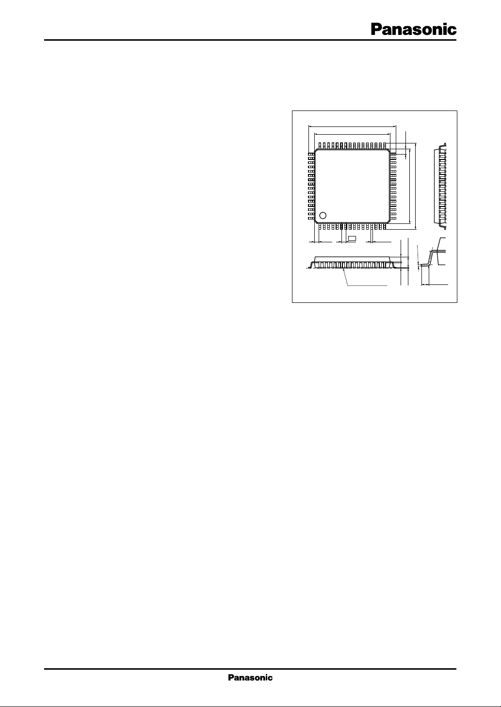
16.2±0.3
14.0±0.2
48 33
49
64
116
0.8
(1.0) 0.35
Seating plane
(1.0)
32
17
+0.10
–0.05
1.95±0.20.1±0.1
0.9±0.1 0.9±0.1
QFS064-P-1414
Unit: mm
16.2±0.3
14.0±0.2
+0.10
–0.05
.15
0
0.55±0.2
■ Applications
• Hi-vision TV, wide TV, projection TV, plasma display
panel (PDP)
1
AN5392FBQ ICs for TV
■ Block Diagram
CC
in
in
M
DC regenaration rate
Analog V
Blooming level in
Black peak det.
4847464544
White peak det.
APL det.
R-CLP
G-CLP
41
43
42
B-CLP
40
OSD-R in
39
38
S
OSD-G in
Y
OSD-B in
Y
3736353433
R, G, B limiter in
Spot killer in
VM out
ABL/ACL in
R−Y (S) in
Y (S) in
B−Y (S) in
Y, U, V V
CC
M/S in
CLP (M1) in
R−Y (M1) in
Y (M1) in
B−Y (M1) in
CLP (M2) in
R−Y (M2) in
Y (M2) in
B−Y (M2) in
Y, U, V GND
49
50
51
52
53
54
55
56
57
58
59
60
61
62
63
64
ABL/ACL
block
Y Y G
Video
block
R−Y
Input
block
Chrominance
B−Y
block
R, G, B → Y, U, V
3
1
2
4
5
L GND
2
I
Y-out
B−Y out
R,G,B GND
Matrix
block
R−Y
G−Y
B−Y
block
6
7
8
R-in
R−Y out
CLP (R, G, B) in
G-in
R
B
9
B-in
10
CC
R, G, B V
SW
block
I2C DAC
block
11
in
P
V
R
G
Output
block
B
BLK
block
1213141516
CC
SCL
SDA
L V
2
I
Slave address SW
32
31
30
29
28
27
26
25
24
23
22
21
20
19
18
17
Pulse GND
G-V
CC
G-out
G-GND
B-V
CC
B-out
B-GND
R-V
CC
R-out
R-GND
Analog GND
Pulse V
CC
DI in
CRT mute
Neck mute
R,G,B mute
BLK in
2
ICs for TV AN5392FBQ
■ Pin Descriptions
Pin No. Description
1I
2
L GND
2 R, G, B GND
3B−Y output
4 Y-output
5R−Y output
6 CLP (R, G, B) input
7 R-input
8 G-input
9 B-input
10 R, G, B V
CC
11 VP input
12 Slave address SW
13 SDA
14 SCL
15 I2L V
CC
16 Pulse GND
17 BLK input
18 R, G, B mute input
19 Neck mute input
20 CRT mute input
21 DI input
22 Pulse V
CC
23 Analog GND
24 R-GND
25 R-output
26 R-V
CC
27 B-GND
28 B-output
29 B-V
CC
30 G-GND
31 G-output
32 G-V
CC
Pin No. Description
33 Spot killer input
34 R, G, B limiter input
35 YM input
36 YS input
37 OSD-B input
38 OSD-G input
39 OSD-R input
40 B-CLP filter
41 G-CLP filter
42 R-CLP filter
43 APL detection filter
44 White peak detection filter
45 Black peak detection filter
46 Blooming level input
47 Analog V
CC
48 DC regenaration rate
49 VM output
50 ABL/ACL input
51 R−Y (S) input (Pr (S) input)
52 Y (S) input
53 B−Y (S) input (Pb (S) input)
54 Y, U, V V
CC
55 M/S input
56 CLP (M1) input
57 R−Y (M1) input (Pr (M1) input)
58 Y (M1) input
59 B−Y (M1) input (Pb (M1) input)
60 CLP (M2) input
61 R−Y (M2) input (Pr (M2) input)
62 Y (M2) input
63 B−Y (M2) input (Pb (M2) input)
64 Y, U, V GND
3
AN5392FBQ ICs for TV
■ Absolute Maximum Ratings
■ Absolute Maximum Ratings
Parameter Symbol Rating Unit
Supply voltage V
Supply current I
2
Power dissipation
*
Operating ambient temperature
1
Storage temperature
Note)*1: Except for the operating ambient temperature and storage temperature, all ratings are for Ta = 25°C.
2: The power dissipation PD shown is for the independent IC without a heat sink in the free air at Ta = 70°C.
*
*
CC
CC
1
*
■ Recommended Operating Range
Parameter Symbol Range Unit
V
CC1
V
CC2
I
CC1
I
CC2
P
D
T
opr
T
stg
10.0 V
5.6
70.0 mA
34.0
685 mW
−20 to + 70 °C
−55 to + 150 °C
Supply voltage V
■ Electrical Characteristics at V
CC1
V
CC2
= 9 V, V
CC1
= 5 V, Ta = 25°C
CC2
8.1 to 9.9 V
4.5 to 5.5
Parameter Symbol Conditions Min Typ Max Unit
DC characteristics
Circuit current 1
*
I
CC1
V
CC1
= 9 V, V
= 5 V 395163mA
CC2
1
No signal input
1
Circuit current 2
*
I
CC2
V
CC1
= 9 V, V
= 5 V 202530mA
CC2
No signal input
Y-system
Video voltage gain AY
Input: Sine wave 0.2 V[p-p] 4.7 5.6 6.7 Times
G
f = 1 MHz, contrast: max.
Video voltage gain ∆AY Ratio between R,G and B −2.5 0 +2.5 dB
variation amount Drive: typ.
Frequency characteristics f
Input: Sine wave 0.2 V[p-p] −6 −3 +1dB
Y
f = 30 MHz, contrast: max.
Typical output pedestal DC
Brightness variable range V
Contrast ratio A
APL detection voltage V
Brightness: typ. 2.6 3.0 3.4 V
P
Brightness: min. → max. 1.8 2.2 2.6 V
BR
Contrast: min. → max. 25 30 dB
CON
Input: Total white 0.7 V[0-p] 0. 7 1.0 1.3 V
APL
APL detection pin 43 voltage
APL detection ratio ∆
Input: Total white 0.7 V[0-p] → 0.35 V[0-p]
APL
0.46 0.54 0.66 Times
APL detection pin 43 voltage ratio
Note)*1: I
is a total amount of the current flowing through pin 10, pin 26, pin 29, pin 32, pin 47 and pin 54.
CC1
I
is a total amount of the current flowing through pin 15 and pin 33.
CC2
4
ICs for TV AN5392FBQ
■ Electrical Characteristics at V
= 9 V, V
CC1
= 5 V, Ta = 25°C (continued)
CC2
Parameter Symbol Conditions Min Typ Max Unit
Y-system (continued)
DC regeneration ratio 1 DC
Input signal: APL 10% → 90%, 96 102 107 %
1
APL det. pin 0 V
DC regeneration ratio 2 DC
Input signal: APL 10% → 90%, 65 75 85 %
2
DC regeneration SW/on, polarity: −
DC regeneration ratio 3 DC
Input signal: APL 10% → 90%, 115 125 1 3 5 %
3
DC regeneration SW: On, polarity: +
Output blooming level V
Blooming DC = 3.8 V, 5.7 6.7 7.7 V
BL
pin 43: 0 V, brightness: max.
Output blooming level ∆V
Blooming DC = 3.8 V → 4.2 V, −1.18 − 0.93 − 0.68 V
BL
variation amount pin 43: 0 V, brightness: max.
2
White gradation correction 1
*
Yγ
Gain: max., level: typ. → max. 9.0 14 18.0 %
1
White gradation SW: On
White gradation correction 2
Yγ
Gain: max., level: typ. → min. −24 −18 −12 %
2
2
*
White gradation SW: On
Black extension Y
3
characteristics 1
*
Black extension Y
3
characteristics 2
*
Black extension Y
3
characteristics 3
*
Black extension Y
4
characteristics 4
*
Black extension Y
4
characteristics 5
*
Black extension Y
4
characteristics 6
White character correction 1
*
2
*
V
Output amplitude: 0 V[p-p] − 0.1 0 +0.1 V
BL1
Level: typ., gain: min. → max.
Output amplitude: 1.0 V[0-p] − 0.49 − 0.37 − 0.25 V
BL2
Level: typ., gain: min. → max.
Output amplitude: 2.2 V[0-p] − 0.1 0 +0.1 V
BL3
Level: typ., gain: min. → max.
Black detection: Open → 3 V −1.10 − 0.82 − 0.55 V
BL4
Level: typ., gain: typ.
Black detection: Open → 3 V −2.00 −1.55 −1.00 V
BL5
Level: typ., gain: max.
Black detection: Open → 3 V − 0.48 − 0.30 − 0.12 V
BL6
Level: min. → max., gain: typ.
Blooming DC adjustment 10.0 25.0 40.0 %
W1
Level: max., gain: min. → typ.
2
White character correction 2
*
V
Blooming DC adjustment −9.3 0 9.3 %
W2
Level: min., gain: min. → max.
White character correction off
W
OFFPR
, PB input: +0.2 V[p-p] − 0.2 0 +0.2 V
2
*
Level: max., gain: min. → max.
5
ABL off
*
V
ABL1
ABL/ACL pin: 7.5 V − 0.1 0 +0.1 V
Level: min., gain: min. → max.
5
ABL start 1
*
V
ABL2
ABL/ACL pin: 3 V 0.28 0.39 0.50 V
Level: min. → max., gain: max.
Note)*2: Control a blooming DC voltage (pin 46)
3: Black gradation SW: On
*
4: Black gradation SW: On, brightness: max.
*
5: ABL SW: On, brightness: max.
*
5
AN5392FBQ ICs for TV
■ Electrical Characteristics at V
= 9 V, V
CC1
= 5 V, Ta = 25°C (continued)
CC2
Parameter Symbol Conditions Min Typ Max Unit
Y-system (continued)
ABL start 2
*
V
ABL3
ABL/ACL pin: 3 V − 0.84 − 0.64 − 0.44 V
5
Level: min., gain: min. → max.
5
ABL gain 1
*
A
ABL/ACL pin: 5 V → 3 V − 0.48 − 0.37 − 0.26 V
ABL
Level: typ., gain: max.
6
ACL off
*
A
ACL1
ABL/ACL pin: 7.5 V −50+5%
Level: min., gain: min. → max.
ACL start 1
*
A
ACL2
ABL/ACL pin: 3 V 10 20 30 %
6
Level: min. → max., gain: typ.
6
ACL start 2
*
A
ACL3
ABL/ACL pin: 3 V −45 −35 −25 %
Level: min., gain: min. → typ.
6
ACL gain 1
*
A
ACL4
ABL/ACL pin: 5 V → 3 V −34 −22 −10 %
Level: typ., gain: typ.
Color difference-system
Color difference voltage gain
G
Input: Sine wave 0.2 V[p-p] 9.5 11.4 13.7 Times
R
7
*
f = 1 MHz, R−Y in → R-out
Color difference frequency fc Input: Sine wave 0.2 V[p-p] − 6 − 3 + 2dB
7
characteristics
B−Y axis gain adjusting range G
NTSC 1
B−Y axis gain adjusting range G
NTSC 2
B−Y axis gain adjusting range G
*
HD 1
B−Y axis gain adjusting range G
*
HD 2
Tint variable range T
*
7
*
7
*
7
7
f = 10 MHz
B−Y gain: min., brightness: max. 0.28 0.45 0.61 Times
B-Y1
Tint SW: NTSC
B−Y gain: max., brightness: max. 1.00 1.25 1.60 Times
B-Y2
Tint SW: NTSC
B−Y gain: min., brightness: max. 0.50 0.78 1.18 Times
B-Y3
Tint SW: HD
B−Y gain: max., brightness: max. 1.18 2.00 2.80 Times
B-Y4
Tint SW: HD
Tint: min. → max. ± 33 ± 48 ± 68 °
C
B−Y gain, drive RB: Adjustment
7
Color control
*
C
Color: typ. → max. 3 6 9 dB
CON
Contrast: typ.
7
Color residue
*
C
Color: min., B−Y gain: max. − 50 0 +50 mV[p-p]
MIN
Contrast: max.
7
R−Y angle adjusting range
Note)*5: ABL SW: On, brightness: max.
6: ACL SW: On
*
7: Adjust tint, drive R, B.
*
*
θ
R−Y axis: min. → max. 10 17 24 °
R
6
ICs for TV AN5392FBQ
■ Electrical Characteristics at V
= 9 V, V
CC1
= 5 V, Ta = 25°C (continued)
CC2
Parameter Symbol Conditions Min Typ Max Unit
Color difference-system (continued)
Matrix ratio M1 Tint SW: HD 0.23 0.30 0.35 Times
7
(G−Y/R−Y) HD
*
G−Y matrix: HD
Matrix ratio M2 Tint SW: NTSC 0.38 0.51 0.58 Times
7
(G−Y/R−Y) NTSC 1
*
G−Y matrix: NTSC 1
Matrix ratio M3 Tint SW: NTSC 0.26 0.34 0.40 Times
7
(G−Y/R−Y) NTSC 2
*
G−Y matrix: NTSC 2
Matrix ratio M4 Tint SW: NTSC 0.26 0.34 0.40 Times
7
(G−Y/R−Y) NTSC 3
*
G−Y matrix: NTSC 3
Matrix ratio M5 Tint SW: HD 0.07 0.10 0.13 Times
7
(G−Y/B−Y) HD
*
G−Y matrix: HD
Matrix ratio M6 Tint SW: NTSC 0.15 0.19 0.23 Times
7
(G−Y/B−Y) NTSC 1
*
G−Y matrix: NTSC 1
Matrix ratio M7 Tint SW: NTSC 0.22 0.28 0.34 Times
7
(G−Y/B−Y) NTSC 2
*
G−Y matrix: NTSC 2
Matrix ratio M8 Tint SW: NTSC 0.13 0.17 0.21 Times
7
(G−Y/B−Y) NTSC 3
*
G−Y matrix: NTSC 3
OSD
8
input threshold voltage
Y
S
*
Y
Pin 36 > 2.1 V: OSD 0.9 1.5 2.1 V
STH
Pin 36 < 0.9 V: Main & sub
8
M/S input threshold voltage
*
M/S
Pin 55 > 2.1 V: Sub 0.9 1.5 2.1 V
TH
Pin 55 < 0.9 V: Main (M1, M2)
8
input threshold voltage
Y
M
*
Y
Pin 35 > 2.1 V: Half tone 0.9 1.5 2.1 V
MTH
Pin 35 < 0.9 V: Main & sub
CLP input threshold voltage CLP
Pin 56, 60 (main, sub, OSD) 0.9 15 2.1 V
TH
Pin 6 (RGB)
Pulse width can be clamped W
Pin 56, 60 (main, sub, OSD) 0.8 µs
M
Pin 6 (RGB)
OSD gain G
Input: Sine wave 0.2 V[p-p] 5.0 6.0 7.2 Times
OSD
f = 1 MHz, YS pin: 5 V
OSD frequency characteristics f
OSD
Input: Sine wave 0.2 V[p-p] −7 −3 +1dB
f = 30 MHz, YS pin: 5 V
OSD contrast ratio 1 OSD
Contrast: max. → typ. −3 −1 +1dB
C1
YS pin: 5 V
OSD contrast ratio 2 OSD
Contrast: typ. → min. −16 −11 −7dB
C2
YS pin: 5 V
Note)*7: Adjust tint, drive R, B
8: SW priority: YS > M/S > M1/M2 (I2C), YS: YM is valid at low.
*
7
 Loading...