

Panasonic AN5337K Datasheet

ICs for TV
■ Overview
The AN5337K is suitable for processing of video, chroma, RGB, synchronization, and deflection signals of
NTSC system. It incorporates an I2C bus controller.
■ Features
•
Video : Wide bandwidth filter, adjustable preshoot and
overshoot, adjustable aperture control, ABL input
•
Chroma : ACC filter, color difference output
•
RGB : Color difference input, RGB output
•
Synchronization : Synchronous BLK input/output,
adjustable AFC1 time-constant, adjustable horizontal
center
•
Deflection : Generation of parabola waves and saw-
tooth waves, distortion correction
AN5337K
NTSC Video Signal Processor IC
(15.24)
3 to 15˚
13.7±0
0.25
+
0.2
– 0.05
47.7±0.3
(0.7)
1.778
0.5±0.1
1.0±0.25
3.85±0.3
(3.3)
52-Pin Shrunk DIL-Plastic Package (SDIP052-P-0600A)
Unit : mm
ICs for TV
AN5337K
1
2
9 11 12
20
21
22
23
24
25
26
27
28
29
30
31
32
33
34
353637
38
39
40
41
42
43
44
45
46
47
48
49
50
51
3 4 5 6 7
8
10 13 14 15 16 17 18 19
52
(4)
(4)
White character Slice
White character Compensation
Demodulate Shift
(5)
Demodulate Gain
(6)
Drive
On Screen
R
Cut off
R
Cut off
(R Clamp)
On Screen
G
Cut off
G
Cut off
(G Clamp)
On Screen
B
Cut off
B
Cut off
B Clamp
Cut off
BLK
Drive
(Pulse)
On Screen
Clamp
(2)
Clamp
(1)
TINT
(2)
TINT
(1)
DEMAXIS
(2)
DEMAXIS
(1)
Drive
R
Drive
G
Drive
(B)
WHITE
RGB
MATRIX
(1)
RGB
MATRIX
(3)
RGB
MATRIX
(2)
On Screen
BLK
A
CC
Amp. 1
A
CC
Amp. 2
Bias 2
DEMOD
A
CC
Det.
Phase
Shift
Color
Track
APC
Killer
VCO
Y delay
line
Apacon
delay
50ns
Apacon
delay
125ns
Apacon
delay
175ns
Apacon
delay
50ns
Sharpness Y Clamp
Color
Control
Color
Control
G –Y
MATRIX
Contrast
Control
IRE
Voltage
Imp.trs Bright
V/I Converter
Bright
Control
APL Det.
Bright
min.Det.
White
max.Det.
IRE Gain
gCont
Brt. Cont
30/60
Cont Gain
Under 60
Cont
Black
APL
60 IRE
Det.
SW
Bright
Pedesta1
Corner
Control
Ramp
EW Amp.
V Amp.
Parabola
H Sync.
Sep.
H.V. Sync.
Sep.
Lock Det.
Neck
Shut/Hold
Down
Power
ON/OFF
AFC 1
V Count down
VCO
R Count
down
S.C.P
BG P2
AFC 2
AFC Gain
(2)
BLK PLS
(1)
Service SW
(1)
Vertical Place
(6)
Palabolic
Correction
EW Contrast2 (3+SW)
EW Contrast1
(3+SW)
Black Slice
(31SW)
Service SW
(1)
DC tra
(1)
Bright
(8)
Voltage
γ Gain
(4)
γ Level
(4)
Color/Black
Compensation
Change (1)
Y delay line
(1)
Apacon delay
(1)
Contrast
(7+1)
Pre over
sharpness
(7)
Y Clamp
Color track ON/OFF
(1)
TINT
(7)
Color
(7+1)
G–Y Ratio
Drive 1
(7+SW)
Cut off R
(8+2)
Cut off G
(8)
Cut off B
(8 + 2)
Mute
(1)
Drive 2
(7+SW)
Killer Filter
CW out
APC Filter
3.58 VCO
B–Y out
R–Y out
V/C/RGB
R–Y in
B–Y in
R in
G in
B in
Ys in
EHT in
B outG outR outV
CC
9VParabolaV outCorner
RAMPAGC
SCL
IIC GND
SDA6.3VH out
X–RAY–REFX–RAYAFC 22f
H
VCO
Sync.DEF
GND
AFC 1
V Pulse
FBPin
S.C.P out
S.C.P inAFC FBP in
Lock Det.
Sync.in
Sync.in
Y in
ACL
Black min.Det.
White max.Det.
APL Det.
Bluming level
ABL
5V C in
Color Track
I
2
C/DAC
GND
Black Gain
(4)
SCP change
(1)
Vertical Linearity (6)
Vertical Amplitude (7)
Vertical S character (6)
Vertical EHT (4)
EW Parabola (6)
Horizontal – EHT (4)
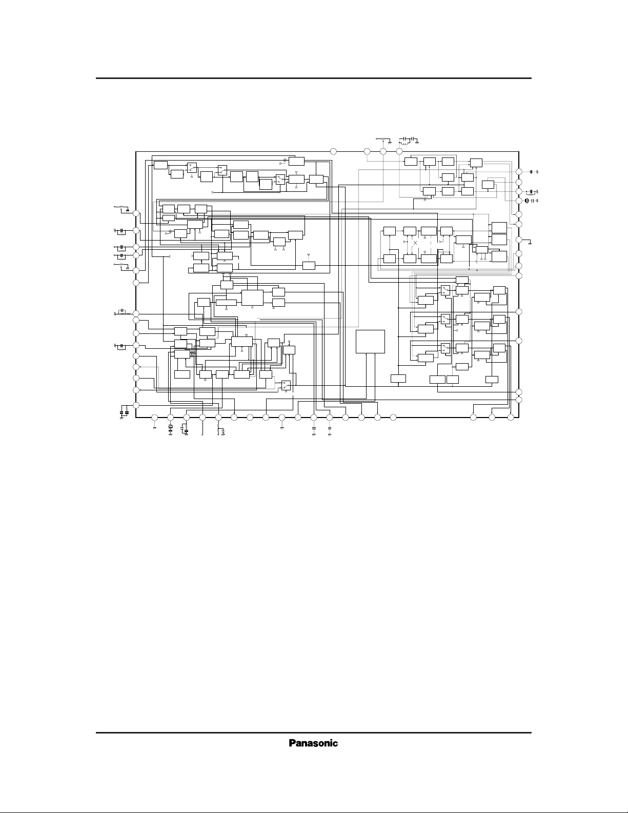
■ Block Diagram

ICs for TV
AN5337K
Pin No.
Pin name
Pin No.
Pin name
1
2
3
4
5
6
7
8
9
10
11
12
13
14
15
16
17
18
19
20
21
22
23
24
25
26
27
28
29
30
31
32
33
34
35
36
37
38
39
40
41
42
43
44
45
46
47
48
49
50
51
52
Sync. Def GND
503kHz VCO
AFC2 filter
High voltage det. input (X–ray)
High voltage det. ref. voltage
Horizontal drive pulse output
Horizontal power supply (HV
CC
)
I
2
C SDA input
I
2
C GND
I
2
C SCL input
Reference ramp waveform AGC
Reference ramp waveform generation
Corner slice level
Ver. deflection saw-tooth output
EW output
9V power supply (V
CC
1
)
R output
G output
B output
EHT voltage detection
Ys input
On-screen B input
On-screen G input
On-screen R input
B –Y input
R –Y input
V/C/RGB GND
R –Y output
B –Y output
3.58MHz VCO
Chroma APC filter
VCO output
Killer filter
Color track filter
ABL input
Chroma input
5V power supply (V
CC2
)
Blooming level input
Filter for APL detection
Filter for white detection
Black det. filter/color control
ACL input
Y signal input
V sync. sep filter
H sync. input
V sync. input
Lock det. filter
Sand castle pulse input/FBP input for AFC
Sand castle pulse output
Flyback pulse (FBP) input for BLK
V pulse output
AFC1 filter
■ Pin Descriptions
V
CC1
V
CC2
I
CC1
(I16)
I
CC2
(I37)
I
7
Supply current
Power dissipation
Note 2)
Operating ambient temperature
Note 1)
Storage temperature
Note1)
P
D
T
opr
T
stg
mA
mW
˚C
˚C
Parameter Symbol Rating Unit
■ Absolute Maximum Ratings
9.6
5.6
113
89
26
Supply voltage
1481
–20 to + 70
–55 to +150
Note 1) Ta= 25˚C except operating ambient temperature and storage temperature.
Note 2) Allowable power dissipation of the package at Ta=70˚C.
V
Parameter Symbol Range
Operating supply voltage range
8.5V to 9.0V to 9.5V
V
CC1
V
16–1, 9, 27
V
CC2
V
37–1, 9, 27
Operating supply current range
I
7
15mA to 20mA to 25mA
4.5V to 5.0V to 5.5V
■ Recommended Operating Range (Ta= 25˚C)
ICs for TV
AN5337K
Parameter Symbol Condition min typ max Unit
I
16
I
37
V
45–1
V
46–1
V
43–27
V
35–27
V
42–27
V
38–27
V
36–27
V
29–27
V
28–27
74
59
0.8
0.8
2.7
2.5
2.5
2.2
1.5
2.3
2.3
106
83
1.8
1.8
3.7
3.5
3.5
3.2
2.5
3.3
3.3
mA
mA
V
V
V
V
V
V
V
V
V
V
CC1
: 9V, V
CC2
: 5V
Pin7 with 380Ω 12V
V
CC1
: 9V, V
CC2
: 5V
Pin7 with 380Ω 12V
V
CC1
: 9V, V
CC2
: 5V
Pin7 with 380Ω 12V
V
CC1
: 9V, V
CC2
: 5V
Pin7 with 380Ω 12V
V
CC1
: 9V, V
CC2
: 5V
Pin7 with 380Ω 12V
V
CC1
: 9V, V
CC2
: 5V
Pin7 with 380Ω 12V
V
CC1
: 9V, V
CC2
: 5V
Pin7 with 380Ω 12V
V
CC1
: 9V, V
CC2
: 5V
Pin7 with 380Ω 12V
V
CC1
: 9V, V
CC2
: 5V
Pin7 with 380Ω 12V
V
CC1
: 9V, V
CC2
: 5V
Pin7 with 380Ω 12V
V
CC1
: 9V, V
CC2
: 5V
Pin7 with 380Ω 12V
90
71
1.3
1.3
3.2
3.0
3.0
2.7
2.0
2.8
2.8
Circuit current
Circuit current
Synchronous input terminal voltage
Synchronous input terminal voltage
Video input terminal voltage
ABL input terminal voltage
ACL input terminal voltage
Chroma input terminal voltage
B –Y output terminal voltage
R –Y output terminal voltage
HV
CC
5.9 6.7 V
V
CC1
: 9V, V
CC2
: 5V
Pin7 with 380Ω 12V
6.3
f
HO
frequency difference when
other supply OFF→ON
Horizontal stabilized supply voltage
Constant voltage operation resistor
Horizontal free-run oscillation frequency (1)
RHV
CC
f
HO–1
I
7
· 15 to 25mA 30 Ω
16.05
200
kHz
Hz
f
HO
variation to rising power supply
15.45015.75
100
Horizontal output pulse duty τ
HO
34.4 40.6 %37.5
∆f
HO
V
CC3
V
fH (S)
5.2 V
Horizontal output starting voltage
Horizontal output level
Horizontal pull-in range
H center variable range (1)
H center variable range (2)
Lock detector output voltage (1)
Lock detector output voltage (2)
Lock detector output voltage (3)
Shut-down operation voltage
Burst gate pulse width
V
fH
f
PH
TDH
T
DH
V
47–M
V
47–L
V
47–T
V
Hth
T
BGP
3.4 V
2.4
±400
1.8
– 3.0
5.1
– 0.1
7.6
2.65
1.8
2.9
f
HO
=15.73kHz
Phase lead at 1A[10]→ [00]
Phase lead at 1A[10]→ [1F]
Synchronized
Not synchronized
Shut down
Vref (= Pin5) = 6.2V
Sandcastle pulse output
Hz
µs
µs
V
V
V
V
µs
V
BGP
V
HBLK
V
VBLK
4.0
2.7
1.2
3.2
–1.6
6.5
0.5
9.0
2.95
3.2
V
V
V
2.5
– 2.3
5.8
0
8.3
2.8
2.5
V
CC
: typ.
VCC : typ.
VCC : typ.
Sandcastle pulse output level (BGP)
Sandcastle pulse output level (HBLK)
Sandcastle pulse output level (VBLK)
f=10k to 20kHz when horizontal
oscillation output is more than 1V
P–P
Blooming level terminal voltage
4.6
3.3
1.8
4.3
3
1.5
DC Characteristics
Horizontal Signal Processing
Vertical Signal Processing
Vertical output pulse width
Vertical output level
Vertical output free-run frequency
Vertical blanking pulse width
τ
VO
V
51H
f
VO
τ
VBLK
360
1.3
58.8
1.09
380
1.8
60
1.12
400
2.3
61.2
1.15
µs
V
Hz
ms
■ Electrical Characteristics (Ta= 25±2˚C)
ICs for TV
AN5337K
Parameter Symbol Condition min typ max Unit
17
– 2.5
–1.5
11.5
11.5
3.5
23
2.5
1.5
17.5
17.5
8.5
200
dB
dB
dB
dB
dB
dB
mV
20
0
0
14.5
14.5
6
30
V
BR
– 6
–5
Video voltage gain
Video voltage gain relative ratio
Video voltage gain relative ratio DL
Sharpness 1
Sharpness 2
ACL characteristics
ABL characteristics
∆yACL
∆Y
ABL
Pin42 3V→3.5V
Pin35 2.7→3.5V
14
4.1
dB/V
V/V
11
3.4
Y frequency characteristics 1
Y frequency characteristics 2
Y delay line : ON
Y delay line : OFF
Contrast : min.
Cont : max. Sharp : min.
Ratio between channels
Drive : typ.
Y delay line ON/OFF
f=4MHz, aper. con. SW : 00
f=3MHz, aper. con. SW : 02
Y signal delay time 1
Y signal delay time 2
8
2.7
Black extention range
Black extention gain
∆YBL1
∆YBL2
– 0.1
1.6
0.1
2.3
V
V
0
1.95
Y
G
0.08 0.28 V0.18
0.5
3.2
1.2
4.6
0.85
3.9
Cut-off : 80
– 0.12
0.12
V
0
Input : full black, Pin
41 : 5V→
CR filter
Input : full black, Pin41 : 3V
Black gain : min.→max.
Pedestal level (standard)
White γ gains : max.
White γ level : min. to max.
Blooming
DCPin38 : 0.5V→4.5V
Black level : min.
Adjust output 0.8V
P–P
by contrast.
After that make black level be maximum.
Pin41 ; 5V, adjust Y output to 2.7V
P–P
by contrast,
after that connect Pin45 to CR filter.
Contrast control range max.
Contrast control min. value
Brightness variable range
AY
G
AY
AY
Gd1
AG
(SH)1
AG
(SH)2
AG
(CON)
τ
DL1
τ
DL2
∆y1 (Y)
∆y2 (Y)
g correction range min. to max.
Blooming level variation range
Black extention range
Y
γ
∆YBLM
∆YBL4
Black extention start point ∆YBL3
260
160
2.0
325
205
– 3
–2
2.4
+1
+2
390
250
2.8
dB
dB
ns
ns
V
V
V
ACC characteristics 1
ACC characteristics 2
Killer tolerance
Chroma Signal Processing
Killer tolerance hysteresis
Demodulation output amplitude B–Y
ACC1
ACC2
e
k
Color bar signal
(burst 300mV
P–P
)
Color bar signal
(burst 18mV
P–P
)
Color bar burst
0dB=150mV
P–P
Color bar signal burst
0dB=150mV
P–P
Color bar signal
(burst 150mV
P–P
)
e
k
e
OB
–1
– 4
– 48
+1
+1
– 38
dB
dB
dB
0
–1.5
– 43
+ 4 dB+ 2
1.04 1.34 1.64
V
P–P
e
OR
R/B
0.82
0.48
1.32
0.64
V
P–P
times
1.07
0.56
Demodulation output amplitude R–Y
Demodulation output ratio
Color bar signal
(burst 150mV
P–P
)
Rainbow signal R–Y/B–Y
output ratio
Sharp : min. Cont : typ.
DC restoration rate 1
DC restoration rate 2
TDC1
TDC2
3.0
90
96
3.7
96
103
4.4
102
110
V
%
%
y
G (CON)min.
No input, Bright : min.→max.
APL10→ 90%
DC transmission range : – direction
APL10 → 90%
DC transmission range : + direction
10MHz attenuation range
DL for f=3MHz : ON
10MHz attenuation range
DL for f=3MHz : OFF
Y Signal Processing
■ Electrical Characteristics (cont.) (Ta= 25±2˚C)
ICs for TV
AN5337K
Parameter Symbol Condition min typ max Unit
Demodulation angle B–Y
Demodulation angle R–Y
∠B
∠R
–5
83
593degree
degree
0
88
Color residue
e
killer
50 mV
P–P
[2F]
[4A]
[3A]
Tint variable range max.
*
Tint variable range min.
*
R–Y demodulation axis variable range
*
B–Y ratio variable range (1) *
B–Y ratio variable range (2)
*
G–Y/R–Y ratio (1)
*
G–Y/R–Y ratio (2)
*
G–Y/B–Y ratio (1)
*
G–Y/B–Y ratio (2)
*
∆θ
1
∆θ
2
∆θ
Dem
AB–Y min.
AB–Y min.
eG/e
R2
eG/e
R1
eG/e
B2
eG/e
B1
Tint : typ.→max.
Tint : typ.→min.
Demodulation axis : min.→max.
Demodulation ratio
: typ.→
min.
Demodulation ratio
: typ.→
max.
G–Y ratio change-over : 02
G–Y ratio change-over : 01
G–Y ratio change-over : 02
G–Y ratio change-over : 01
40
–37
16
1.25
0.23
0.37
0.12
0.18
39
0.25
1.75
0.37
0.57
0.28
0.36
degree
degree
degree
times
times
times
times
times
times
65
–50
28
0
1.5
0.3
0.47
0.2
0.27
RGB Signal Processing
Killer filter terminal grounded
by 20kΩ
Demodulation output residual carrier
APC pull-in range Low
APC pull-in range High
CW output amplitude
Free-run frequency
No signal input
Burst frequency variation
Burst frequency variation
Shift from 3.579545MHz
Pin25 356mV
P–P
Pin26 200mV
P–P
DAC value
where R.B outputs are coincident
Tint center
θ
t
600
– 600
800
0
1100
200
500
–500
600
–200
Bright : typ. cut-off
Cont : typ.
Color : typ.→max.
Cont : typ.
Color : typ.→max.
Cont : typ.
Color : typ.→min.
Drive SW : 00→04
Drive : min.→max.
Cut off SW
Cut off : min.→max.
Cut-off min. to max.
E
BLK
0.7
3.4
3.5
4
1.6
0.6
1.5
6.6
50
8.5
8
2.6
1.6
V
dB
mV
dB
dB
V
V
1.1
5.0
25
6
6
2.1
1.1
A
B (CON)
A
R (DR)
V
(CO)
V
(CO)G
A
B–Y
cl
max.
A
B–Y
cl
min.
Color control range max.
*
Color control min. value
*
Color difference contrast variable range
*
Drive control range
Cut-off R · B control range
Cut-off G control range
RGB output blanking voltage
50 mV
P–P
Hz
Hz
mV
P–P
Hz
Deflection Signal Processing
8
0
0.1
– 6
12
3.5
0.5
+1
dB
dB
V
P–P
dB
10
1.5
0.3
– 3
On-screen voltage gain
On-screen contrast range
On-screen contrast min. value
On-screen frequency characteristics
A
yG
A
yG (ON)
∆e
Standard vertical output amplitude
Standard EW output amplitude
V
out
V
EW
2.2
1.8
3.0
2.6
V
P–P
V
P–P
2.6
2.2
Ys=1V Contrast ; max.
Ys=1V typ.→max.
A
yG (ON)
min.
0.5V input
Attenuation quantity at f=10MHz
to f=3MHz
Horizontal Signal Processing
(0.2) V
P–P
Hz/˚C
(1.0)
(5.5)
Separable sync. signal
f
HO
ambient temperature dependency
Input : full black sync. level
Ta= –20 to + 70˚C
∆f
HO
Ta
Hz/mV(1.2)
0D [30]
mA(0.83)
b
H
I30 (1)
Horizontal oscillation frequency control sensitivity
AFC1 reference current (1)
V
IN
e
car
fpull
fpull
e
cw
f
co
Note) The characteristics value in parentheses is not a guaranteed value, but reference one on design.
* The state in which R, B amplitudes and G amplitude are made coincident, is come out by means of drive I, II adjustments where
Y signal is inserted to Pin17.
■ Electrical Characteristics (cont.) (Ta= 25±2˚C)

ICs for TV
AN5337K
Parameter Symbol Condition min typ max Unit
(19)
V
CC2
5V±0.5V
V
CC2
5V±0.5V
V
CC2
5V±0.5V
Zener temperature characteristics +1.8mV/deg
V
FBP–1
V
FBP–2
V
V
H center : typ.
Hout rise to FBP center
Horizontal sync. rear edge to
Burst gate pulse front edge
(0.7)
(2.5)
Sandcastle pulse input threshold level
temperature characteristics
FBP input threshold level temperature
characteristics HBLK
FBP input threshold level temperature
characteristics AFCI
T
H–FBP
∆V
48 (Ta)
∆V
50 (Ta)
µs
µs
mV/deg
mV/deg
mV/deg
(0.3)
(1.8)
(0)
(1)
(0.74)
(0.44)
F.B.P slice level (blanking)
F.B.P slice level (AFCI)
F.B.P delay time range
B.G.P start position
Sandcastle pulse output temperature characteristics
X– ray inner reference temperature characteristics
Sandcastle pulse output supply voltage
dependency BGP
Sandcastle pulse output supply voltage
dependency HBLK
Sandcastle pulse output supply voltage
dependency VBLK
∆V
49 (Ta)
(0)
(–1.8)
(1)
mV/deg
V/V
mV/deg
V/V
V/V
Vertical Signal Processing
Vertical BLK phase (WIDE)
Vertical BLK phase (NORMAL)
Neck break operation Pin49 voltage
Vertical BLK pulse width (WIDE)
Y Signal Processing
Contrast variable range
Y output amplitude V
CC
dependency
Y output DC voltage V
CC
dependency
Y noise level
Delay line dynamic range
Y output amplitude ambient temperature dependency R
Y output amplitude ambient temperature dependency G
Y output amplitude ambient temperature dependency B
APL detection voltage
PVBLK (W)
PVBLK
V
49
TVBLK (W)
A
yG (CON)
min.
∆y
G
(VCC)
∆Y
G
(VCC)
VY
NL
V
DLmax
A
APL
∆yR (Ta)
∆y
G
(Ta)
∆y
B
(Ta)
Period from VBLK rise up to
vertical sync. fall down
Period from VBLK rise up to
vertical sync. fall down
Pin5 : 1.5V
Contrast : 00 to 7F
APL 50→100% detection
voltage ratio
–20 to +70˚C
–20 to +70˚C
–20 to +70˚C
(1.5)
(1)
(3.87)
(0.2)
(5.05)
(40)
(0.4)
(0.18)
(7)
(0.7)
(–6)
(–8)
(–6)
(2)
(4)
(50)
ms
ms
V
ms
dB
dB/V
V/V
mV
V
times
%
%
%
AFC1 reference current
(2)
AFC1 reference current
(3)
AFC1 reference current
(4)
I
30 (2)
I
30 (3)
I
30 (4)
0D [20]
0D [10]
0D [00]
(1.33)
(1.83)
(2.33)
mA
mA
mA
Chroma Signal Processing
e0 –V
∆f
CO
–V
(0)
(220)
dB/V
Hz/V
Demodulation output amplitude VCC dependency
VCO VCC dependency
Demodulation output ambient temperature dependency R–Y
Demodulation output ambient temperature dependency B–Y
Burst-chroma ratio tolerance
∆e
R–Y
(Ta)
∆e
B–Y
(Ta)
Burst compression tolerance
for color bar chroma
–20 to +70˚C
–20 to +70˚C
(– 40)
(–3)
(–3)
%
%
%
∆e0 (bst)
Note) The characteristics value in parentheses is not a guaranteed value, but reference one on design.
■ Electrical Characteristics (cont.) (Ta= 25±2˚C)
 Loading...