

ICs for TV
AN5308NK
Single chip IC for color TV (Built-in I2C bus interface)
■ Overview
The AN5308NK is an IC in which NTSC video,
chroma, RGB, sync. and deflection signal processing circuits are integrated on a single chip incorpo-
2
rating I
C bus controller.
■ Features
•
Video block :Built-in wide band width filter,
pre-shoot and over-shoot
amount adjustment, aperture
changeover possible and with
ABL pin
•
Chroma block :Built-in ACC filter and with
color difference output pin
•
RGB block :With color difference signal
input pin and analog RGB
•
Sync. block :With sync. BLK in/output pin,
µ changeover and H center
adjustment possible
•
Deflection block: Built-in screen distortion
correction circuit
■ Applications
•
TV
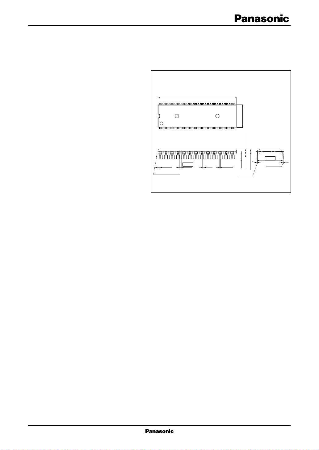
Unit: mm
64 33
132
(1.641)
Seating plane
58.4±0.3
1.778
0.5
+0.1
–0.05
(1.0)
SDIP064-P-0750B
17.0±0.2
3.85±0.2
(3.3)
0.7 min.
0° to 15°
5.2 max.
19.05
0.25
+0.1
–0.05
1
AN5308NK ICs for T V
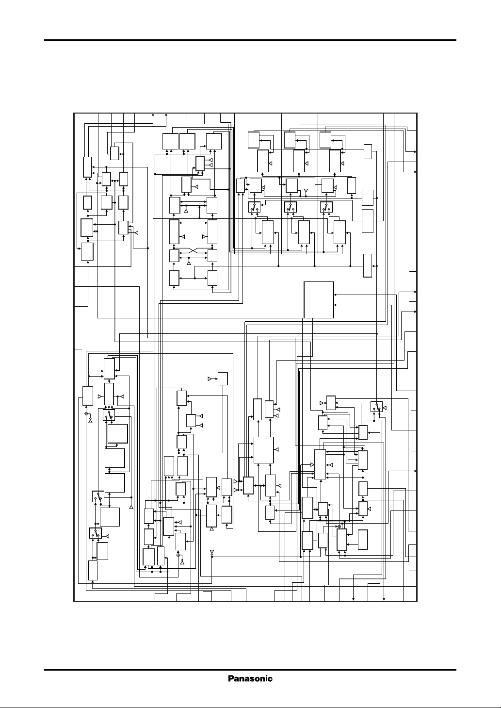
■ Block Diagram
in
S
EHT in
BLK
Drive
(Pulse)
BLK
On Screen
On Screen
S.C.P
down
H Count
VCO
AFC1
Power
On/Off
61
Y
26
(1)
AFC gain
62
25
24
22
21
20
19
18
16
17
15
14
13
12
11
10
SCP selection(1)
9
7
6
5
4
3
2
1
64
63
B-out
G-out
Corner
gain cont.
R-out
9 V
Parabola
9 V
V-out
Feed back
Ramp
AGC
SCL
I2C GND
SDA
6.3 V
H-out
X-ray-ref
X-ray
AFC2
Key stone
filter
2fH VCO
Sync./Def.
GND
Sharpness
control
Color
track
ABL
C-in
5 V
Y -clamp
B-in
Corner
slice vol.
DriveRDrive
R
Cut off
(R-clamp)
Drive1
On Screen
R
(7+SW)
G-in
27
28
29
(8)
(G-clamp)
Cut off G
Mute(1)
G
On Screen
C/DAC
2
I
B
Cut off
Cut off
(8+2)
(B-clamp)
Cut off B
B
Drive
Cut off
Drive2
(7+SW)
B
On Screen
G
Cut off
Cut off
(8+2)
Cut off R
G
Drive
R-in
B−Y in
R−Y in
V/C/RGB
GND
R−Y out
B−Y out
3.58 VCO
APC filter
CW out
Killer filter
31
33
(1)
RGB
G−Y
Color
control
(1)
DEMAXIS
Demodulate
(1)
Tint
Tint
(1)
Clamp
(3)
matrix
matrix
(7+1)
Color
shift(5)
Demodultae
(7)
32
(2)
RGB
matrix
White
G−Y
Ratio
White character slice(4)
White character correction(4)
Color
control
(2)
DEMAXIS
Gain(6)
(2)
Tint
(2)
Clamp
30
Cut o ff
35
36
37
38
40
41
RGB
matrix
VCO
APC
Killer
det.
Bias2 DEMOD
ACC
amp.2
ACC
amp.1
42
shift
Phase
ACC
(1)
track
Color
Color track ON/OFF
43
44
45
49
Y-clamp
control
Contrast
(7+1)
Contrast
Y-clamp
Pre Over
Aperture
Aperture
control
Aperture
line
Y - delay
Sharpness
delay
control
Aperture
delay
control
delay
control
50 ns
delay
line(1)
Y-delay
Sharpness(7)
50 ns
125 ns
125 ns
delay(1)
Aperture control
Bright
lmp.trs
IRE
Voltage
46
Bright
Bright
Voltage1
Burst
IRE
White
min.det.
APL
Pedestal
Bright
47
cont.
γ
gain
max.det.
det.
(1)
DC tra
control
Bright(8)
selection
Color/Black
level correction
cont.
Service SW
48
(1)
(4)
γ level
(4)
γ gain
Black
cont.
Under 60
30/60
cont.gain
(3+SW)
Black slice
(1)
50
SW
gain(4)
det.
60 IRE
APL
Black
51
SW corner(2)
Corner
control
(3)
EW corner 1
52
V-amp.
EW amp.
Parabola
V/I
(1)
Vertical amp. polarity
Vertical
position(6)
Service
Vertical linearity(6)
Vertical amplitude(7)
Vertical S-curve(6) Vertical EHT(4)
EW parabola(6) Horizontal EHT(4)
Converter
Trapezoidal
correction(6)
sep.
Ramp
53
H.V.sync.
sep.
H-sync.
54
55
56
57
SW(1)
(5)
H-center
BGP2
down
V count
det.
Lock
Neck
58
AFC2
BLK PLS
59
(1)
down
Shut/Hold
60
Y-in
ACL
Sync. in
Sync. in
B.P.P. in
APL det.
Blooming level
Black min. det.
White max. det.
Slv. add.
Lock det.
S.C.P. in
S.C.P. out
FBP in
V-pulse
AFC1
2
ICs for TV AN5308NK
■ Pin Descriptions
Pin No. Description
Pin No. Description
1 Sync., Def. GND
2 503 kHz VCO
3 Vertical position transition DAC output
4 AFC2 filter
5 High-tention detection input (X-ray)
6 High-tention detection reference voltage
7 Horizontal drive pulse output
9 Horizontal power supply (H VCC)
10 I2C SDA input
11 I2C GND
12 I2C SCL input
13 Reference ramp wave form AGC
14 Reference ramp wave form generation
15 Corner slice level
16 Sync. 9 V power supply
17 Vertical deflection sawtooth wave output
18 EW output
19 9 V power supply (V
CC1
)
20 R-output
21 Corner gain control
22 G-output
24 B-output
25 EHT voltage detection
26 YS input
27 On-screen B-input
28 Corner slice volume
29 On-screen G-input
30 On-screen R-input
31 B−Y input
32 R−Y input
33 V/C/RGB GND
35 R−Y output
36 B−Y output
37 3.58 MHz VCO
38 Chroma APC filter
40 VCO output
41 Killer filter
42 Color track filter
43 ABL input
44 Chroma input
45 5 V power supply (V
CC2
)
46 Blooming level input
47 APL detection use filter
48 White detection use filter
49 Y-clamp
50 Black detection filter/color control
51 ACL input
52 Y-signal input
53 Slave address changeover
54 V-sync. sep. filter
55 H-sync. input
56 Black detection inhibition pulse input
57 V-sync. input
58 Lock det. filter
59 Sandcastle pulse input
60 Sandcastle pulse output
61 Flyback pulse (FBP) input
62 V-pulse output
63 AFC1 filter
64 Sharpness control output
8, 23, 34, 39 Non-connection
3
AN5308NK ICs for T V
■ Absolute Maximum Ratings
Parameter Symbol Rating Unit
Supply voltage V
Supply current I
Power dissipation (Ta = 70°C) P
1
Operating ambient temperature
1
Storage temperature
Note)*1: Except for the operating ambient temperature and storage temperature, all ratings are for Ta = 25°C.
*
*
CC
CC
D
T
opr
T
stg
■ Recommended Operating Range
Parameter Symbol Range Unit
Supply voltage V
Supply current I
CC1
V
19−1, 11, 33
V
CC2
V
45−1, 11, 33
9
V
CC1
V
CC2
I
(I16+I19) 113 mA
CC1
I
(I45)89
CC2
I
9
9.6 V
5.6
26
947 mW
−20 to +70 °C
−55 to +150 °C
8.5 to 9.0 to 9.5 V
4.5 to 5.0 to 5.5 V
15 to 20 to 25 mA
■ Electrical Characteristics at Ta = 25°C
Parameter Symbol Conditions Min Typ Max Unit
DC characteristics
Supply current I
Supply current I
Sync. input pin voltage V
Sync. input pin voltage V
Video input pin voltage V
ABL input pin voltage V
ACL input pin voltage V
Blooming level pin voltage V
Chroma input pin voltage V
16+19
45
55−1
57−1
7−33
43−33VCC1
51−33VCC1
46−33VCC1
44−33VCC1
V
: 9 V, V
CC1
with 380 Ω
V
: 9 V, V
CC1
with 380 Ω
V
: 9 V, V
CC1
with 380 Ω
V
: 9 V, V
CC1
with 380 Ω
V
: 9 V, V
CC1
with 380 Ω
: 9 V, V
with 380 Ω
: 9 V, V
with 380 Ω
: 9 V, V
with 380 Ω
: 9 V, V
with 380 Ω
: 5 V, pin 9: 12 V 7 4 90 106 mA
CC2
: 5 V, pin 9: 12 V 5 9 71 83 mA
CC2
: 5 V, pin 9: 12 V 0.8 1.3 1. 8 V
CC2
: 5 V, pin 9: 12 V 0.8 1.3 1. 8 V
CC2
: 5 V, pin 9: 12 V 2.7 3.2 3. 7 V
CC2
: 5 V, pin 9: 12 V 2.5 3.0 3. 5 V
CC2
: 5 V, pin 9: 12 V 2.5 3.0 3. 5 V
CC2
: 5 V, pin 9: 12 V 2.2 2.7 3. 2 V
CC2
: 5 V, pin 9: 12 V 1.5 2.0 2. 5 V
CC2
4
ICs for TV AN5308NK
■ Electrical Characteristics at Ta = 25°C (continued)
Parameter Symbol Conditions Min Typ Max Unit
DC characteristics (continued)
B−Y output pin voltage V
31−33VCC1
: 9 V, V
: 5 V, pin 9: 12 V 2.3 2.8 3. 3 V
CC2
with 380 Ω
R−Y output pin voltage V
32−33VCC1
: 9 V, V
: 5 V, pin 9: 12 V 2.3 2.8 3. 3 V
CC2
with 380 Ω
Horizontal signal processing
Horizontal stabilized supply voltage HV
CCVCC1
: 9 V, V
: 5 V, pin 9: 12 V 5.9 6.3 6. 7 V
CC2
with 380 Ω
Constant voltage operating resistance RHVCCI9: 15 mA to 25 mA 30 Ω
Horizontal free-running oscillation f
HO-1
15.434 15.734 16.034 kHz
frequency 1
Horizontal free-running oscillation f
HO−2
At hold down 16.3 16.4 16.8 kHz
frequency 2
Variation of fHO, when supply ∆f
voltage start-up V
Horizontal output pulse duty cycle τH
Horizontal output starting voltage V
HOfHO
CC3
O
fH(S)
frequency difference, when 0 100 200 Hz
other power supply off→on
Hold down off 34.4 37.5 40.6 %
f = 10 kHz to 20 kHz, when horizontal 5.2 V
oscillation voltage is 1 V[p-p] or more
Horizontal output level V
Horizontal pull-in range f
H-center changeable range 1 T
H-center changeable range 2 T
Lock detector output voltage 1 V
Lock detector output voltage 2 V
Lock detector output voltage 3 V
Burst gate pulse width T
Sandcastle pulse output level V
fH
fHO = 15.73 kHz ±400 Hz
PH
Phase lead of 1A[10]→[00] 1.8 2.5 3.2 µs
DH
Phase lead of 1A[10]→[1F] −3.0 −2.3 −1.6 µs
DH
Synchronous 5.1 5.8 6.5 V
58−M
Asynchronous − 0.1 0 0.5 V
58−L
Hold down 7.6 8.3 9.0 V
58−T
Sandcastle output 1.8 2.5 3.2 µs
BGP
VCC: typ. 4.0 4.3 4.6 V
BGP
2.4 2.9 3.4 V
(BGP)
Sandcastle pulse output level V
HBLKVCC
(HBLK)
Sandcastle pulse output level V
VBLKVCC
(VBLK)
Vertical signal processing
Vertical output pulth width τV
Vertical output level V
Vertical output free-running frequency f
Vertical blanking pulse width τ
VBLK
62H
VO
: typ. 2.7 3 3.3 V
: typ. 1.2 1.5 1.8 V
O
360 380 400 µs
3.8 4.3 4.8 V
58.8 60.0 61.2 Hz
1.09 1.12 1.15 ms
5
AN5308NK ICs for T V
■ Electrical Characteristics at Ta = 25°C (continued)
Parameter Symbol Conditions Min Typ Max Unit
Y-signal processing (continued)
Video voltage gain AY
Cont.: max., Sharp.: min. 17 20 23 dB
G
Video voltage gain relative ratio AY Ratio between channels, Drive: typ. −2.5 0 2.5 dB
Video voltage gain relative ratio DL AY
Sharpness 1 AG
Sharpness 2 AG
Contrast control range max. value AG
Contrast control range min. value yG
Brightness changeable amount V
CONmin
Y delay line on/off −1.5 0 1.5 dB
GD1
f = 4 MHz, Aperture control SW: 00 11.5 14.5 17.5 dB
SH1
f = 3 MHz, Aperture control SW: 02 11.5 14.5 17.5 dB
SH2
Sharp.: min., Cont.: typ. 3. 5 6.0 8.5 dB
CON
Contrast: min. 30 100 mV
No input, Bright: min.→max. 3.0 3.7 4.4 V
BR
DC re-generation factor 1 TDC1 APL10%→90% DC transmission 90 96 102 %
amount changeover: − direction
DC re-generation factor 2 TDC2 APL10%→90% DC transmission 96 103 110 %
amount changeover: + direction
Y-signal delay time 1 τ
Y-signal delay time 2 τ
Y-frequency characteristics 1 ∆y
Y delay line: On 260 325 390 ns
DL1
Y delay line: Off 160 205 250 ns
DL2
10 MHz attenuation amount −6 −31dB
1Y
DL: On for f = 3 MHz
Y-frequency characteristics 2 ∆y
10 MHz attenuation amount −5 −22dB
2Y
DL: Off for f = 3 MHz
ACL characteristics ∆y
ABL characteristics ∆y
Pin 51: 3 V→3.5 V 8 11 14 dB/V
ACL
Pin 43: 2.7 V→3.5 V 2.7 3.4 4.1 V/V
ABL
Black extension amount 1 ∆YBL1 Input: Whole black, pin 50: 5 V→ − 0.1 0 0.1 V
CR filter
Black extension gain ∆YBL2 Input: Whole black, pin 50: 3 V 1.60 1.95 2.3 V
black gain: min.→max.
Black extension start point ∆YBL3
Pin 50: 5 V, set contrast to 2.7 V[p-p],
− 0.12 0 0.12 V
after that with pin 50 CR filter
Black extension amount 2 ∆YBL4 Black level: min., set contrast to 0.08 0.18 0.28 V
0.8 V[p-p], after that with pin 50 CR
filter
γ correction amount min. to max. Y
White γ gain: max., white γ gain: 0.50 0.85 1.20 V
γ
min. to max.
Blooming level variation amount ∆YBLM Blooming DC pin 46: 0.5 V→4.5 V 3.2 3.9 4.6 V
Pedestal level (typical) Y
Cut off: 80 2.0 2.4 2.8 V
G
Chroma signal processing
ACC characteristics 1 ACC1 Color bar signal (Burst 300 mV[p-p]) −10 1dB
ACC characteristics 2 ACC2 Color bar signal (Burst 15 mV[p-p]) −4 −1.5 1 dB
6
ICs for TV AN5308NK
■ Electrical Characteristics at Ta = 25°C (continued)
Parameter Symbol Conditions Min Typ Max Unit
Chroma signal processing (continued)
Killer tolerance on eK Color bar burst 0 dB = 150 mV[p-p] −48 −43 −38 dB
Killer tolerance off eK Color bar signal hysteresis 24dB
Detection output amplitude B-Y e
Detection output amplitude R-Y e
Color bar signal (Burst 150 mV[p-p]) 1.04 1.57 2.1 V[p-p]
OB
Color bar signal (Burst 150 mV[p-p]) 0.82 1.26 1.7 V[p-p]
OR
De-modulated output ratio R/B Rainbow signal R−Y/B −Y output ratio 0.48 0.56 0.64 Time
De-modutation angle (B−Y) ∠B −8.0 −2.5 3.0 degree
De-modutation angle (R−Y) ∠R 83 88 93 degree
Color residual e
Detection output residual carrier e
APC pull-in range low f
APC pull-in range high f
CW output amplitude e
Free running frequency f
KILLER
PULL
PULL
Killer filter pin, grounded with 20 kΩ 50
No-signal input 50
CAR
Burst frequency change 500 600 Hz
Burst frequency change −500 −600 Hz
CW
Deviation from 3.579545 MHz −200 0 200 Hz
CO
600 800 1 100
mV[p-p]
mV[p-p]
mV[p-p]
RGB processing circuit
Tint center
*
θ
Pin 31: 356 mV[p-p], pin 32: [2F] [3A] [4A]
T
1
200 mV[p-p], DAC value, when
R, B output are equal
1
Tint variable range max.
Tint variable range min.
R−Y demodulation axis variable ∆θ
1
range max.
*
B−Y ratio variable range 1
B−Y ratio variable range 2
R−Y/B−Y ratio
*
*
1
*
1
*
1
*
1
∆θ
∆θ
AB−Y
AB−Y
Tint: typ.→max. 40 65 degree
1
Tint: typ.→min. −37 −50 degree
2
Demodulation axis: min.→max. 16 28 39 degree
DEM
Demodulation ratio: typ.→min. 0 0.25 Time
min
Demodulation ratio: typ.→min. 1.25 1.50 1.75 Time
min
eR/eB Pin 31: 356 mV[p-p], pin 32: 0.65 0.79 0.94 Time
200 mV[p-p]
G−Y/R−Y ratio 1
G−Y/R−Y ratio 2
G−Y/B−Y ratio 1
G−Y/B−Y ratio 2
*1
1
*
1
*
1
*
eG/eR1G−Y ratio changeover: type2 0.47 0.57 0.67 Time
eG/eR2G−Y ratio changeover: type1 0.27 0.35 0.44 Time
eG/eB1G−Y ratio changeover: type2 0.18 0.27 0.36 Time
eG/eB2G−Y ratio changeover: type1 0.30 0.36 0.42 Time
RGB output blanking voltage E
1
Color control range max.
Color control min. value
*
1
*
A
A
Color difference signal contrast A
1
variable range
*
B−YCLmax
B−YCLmin
B(CON)
Brightness: typ., cutoff 0 .7 1.1 1.5 V
BLK
Cont.: typ., Color: typ.→max. 3.4 5.0 6.6 dB
Cont.: typ., Color: typ.→min. 25 50 mV
Color: typ., Cont.: typ.→max. 3.5 6.0 8.5 dB
Note)*1: Under the condition that pin 52 is adjusted for the Drive I, I I by inserting Y-signal, and R and B-output amplitude equal that
of G-output.
7
AN5308NK ICs for T V
■ Electrical Characteristics at Ta = 25°C (continued)
Parameter Symbol Conditions Min Typ Max Unit
RGB processing circuit (continued)
Drive control range A
Cut-off R.B control range V
Cut-off G control range V
On-screen voltage gain A
On-screen contrast range A
On-screen contrast min. value
A
yG(ON)min
R(DR)
(CO)G
yG(ON)YS
Drive SW: 00→04, drive: min.→max. 4 6 8 dB
Cutoff SW, cutoff: min.→max. 1.6 2.1 2.6 V
CO
Cutoff: min. to max. 0.6 1.1 1.6 V
YS = 1 V, contrast: max. 8 10 12 dB
yG
= 1 V typ.→max. 0 1.5 3.5 dB
0.5 V input 0.1 0.3 0.5 V[p-p]
On-screen frequency characteristics ∆e Attenuation amount of f = 10 MHz −6 −31dB
to f = 3 MHz
Deflection signal processing
Standard vertical output amplitude V
Standard EW output amplitude V
OUT
EW
2.2 2.6 3.0 V[p-p]
1.8 2. 2 2.6 V[p-p]
Color track
Color track off/on variation amount 1 ∆e
1
*
Blue
Color track off/on variation amount 2 ∆e
1
*
Red
Color track off/on variation amount 3 ∆e
1
*
Yellow
C/Y ratio V
B−Y: 1.39 V, R−Y: 1.1 V −160 0 160 mV
BB
After tint color adjustment
Variation amount at color track −100 100 300 mV
BR
On, 0E : 03→04
RY
C/Y
Y: 0.36 V
, C: Color bar typ., 0.285 0.42 0.56 Time
B-W
−350 −200 −16 mV
Color: typ., contrast: typ.
G−Y/Y zero peak ratio at G-output
Note)*1: Under the condition that pin 52 is adjusted for the Drive I, I I by inserting Y-signal, and R and B-output amplitude equal that
of G-output.
• Design reference data
Note) The characteristics listed below are theoretical values based on the IC design and are not guaranteed.
Parameter Symbol Conditions Min Typ Max Unit
Horizontal signal processing
Sync. separation possible input V
Ambient temperature dependence Df
of f
HO
Horizontal oscillation frequency β
control sensitivity
AFC1 reference current 1 I
AFC1 reference current 2 I
AFC1 reference current 3 I
AFC1 reference current 4 I
8
T
63(1)
63(2)
63(3)
63(4)
Input: Whole black sync. level 0.2 1.0 V[p-p]
IN
Ta = −20°C to +70°C 5.5 Hz/°C
HO
a
H
1.2 Hz/mV
0D[30] 0.83 mA
0D[20] 1.33 mA
0D[10] 1.83 mA
0D[00] 2.33 mA
 Loading...