

Panasonic AN5295NK Datasheet
ICs for TV
AN5295NK
3-ch. sound signal processing single chip IC for TV (with I2C bus)
■ Overview
The AN5295NK is a television-use 3-ch. sound signal processing IC which incorporates volume, tone control (L/R/C 3-ch.), and surround sound, sound AGC,
lower sound enforce (L/R 2-ch.) functions. All of the functions (including changeover switch) including external I/
O port can be controlled by I
2
C bus.
■ Features
• 3-ch. of volumes can be controlled independently (max.
attenuation is 75 dB or more)
• Center output can be switched, ether center input or inside L+R signal (for HDTV)
• Lower sound enforce effect (frequency and gain) can be
adjusted with external parts
• With L+R output
■ Applications
• Television
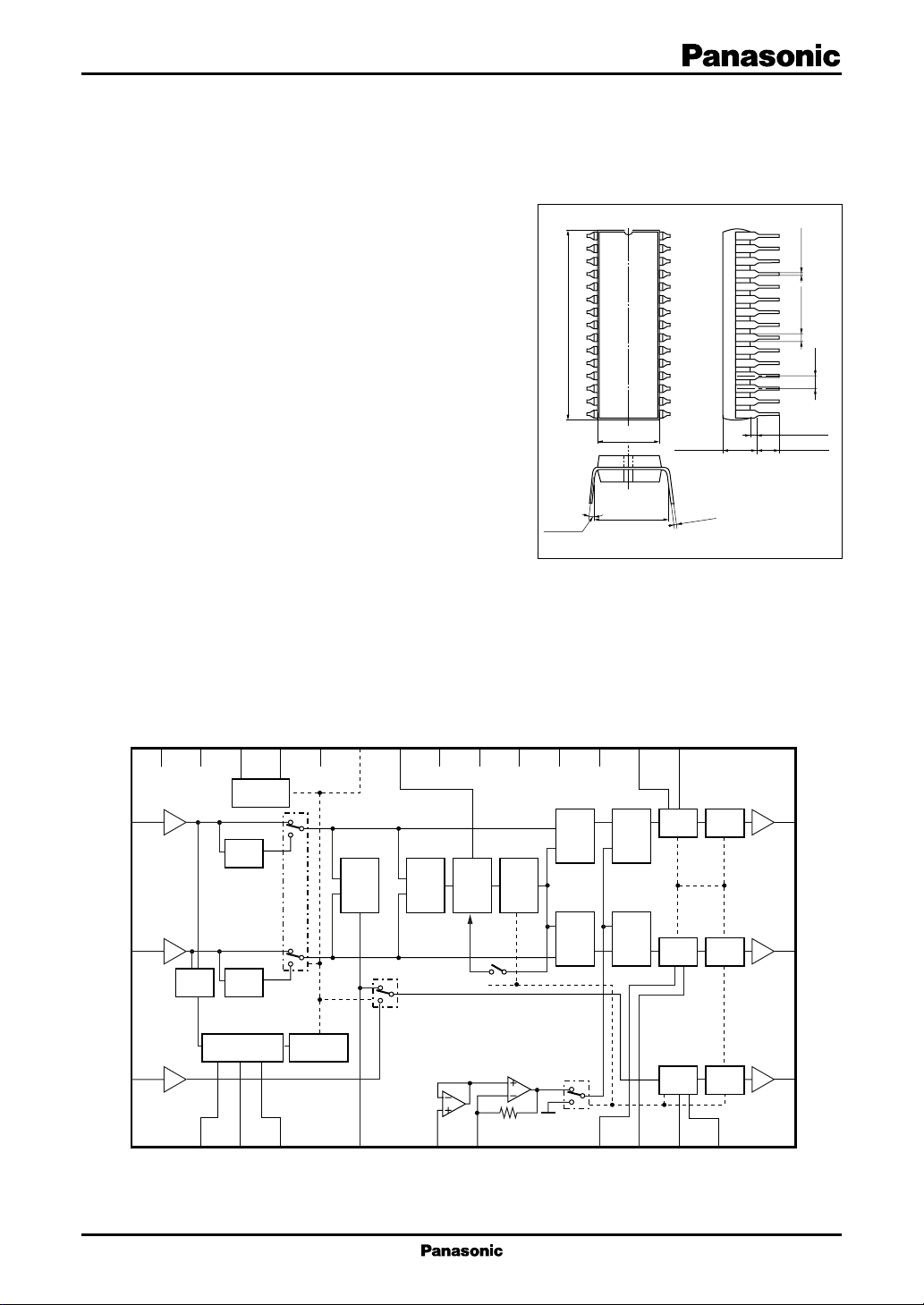
■ Block Diagram
L-In
R-In
30
1
CC
V
29
Buffer
Buffer
GND
2
SDA
15
VCA
VCAL+R
14
I2C
Off
On
Off
On
SCL
2
I
C
REF
V
6
Extension
I/O (H/L)
DAC1
7
17
PS
8
L−RL+R
C-sel
STB
stage
Loop
PS
1st
12
SRV
SLV
13
LPF
amp.1
26.7±0.3
3° to 15°
SCV
16
L+S
R−S
1
15
8.6±0.3
10.16±0.25
STT
25
Add
Add
23
30
16
+0.1
–0.05
0.35
SDIP030-P-0400
LB
LT
22
Vol.+mute
Vol.
Tone
Vol.
Tone
Unit: mm
Buffer
Buffer
1.0±0.25
3.3±0.254.7±0.25
19
11
0.5±0.1
0.9±0.25
1.778
L-Out
R-Out
B-Out/
C-In
Buffer
28
0 dB adj.
3
AGC Adj.
4
LS1
5
ControlLevel sense
LS2
27
ADD
26
B-In
24
B-Gain
Bass add
On
Off
18
Vol.Tone
C-Out
Buffer
9
10
21
20
RB
RT
CB
CT
1

AN5295NK ICs for T V
■ Pin Descriptions
Pin No. Description
1 R-ch. input pin
2 Ground pin
3 AGC 0 dB adjustment pin
4 AGC level sensor-1 pin
5 AGC level sensor-2 pin
6 1/2 VCC pin
7 Phase shift pin
8 L/R/C-ch. bass DAC output pin
9 R-ch. bass fC setting pin
10 R-ch. treble fC setting pin
11 R-ch. output pin
12 R-ch. volume DAC output pin
13 L-ch. volume DAC output pin
14 I2C communication clock pin
15 I2C communication data pin
Pin No. Description
16 C-ch. volume DAC output pin
17 Extension DAC pin 1
18 C-ch. output pin
19 L-ch. output pin
20 C-ch. treble fC setting pin
21 C-ch. bass fC setting pin
22 L-ch. treble fC setting pin
23 L-ch. bass fC setting pin
24 Bass mix. gain adjustment pin
25 L/R/C-ch. treble DAC output pin
26 Bass detection LPF ope.-amp. input pin
27 L+R add after AGC output pin
28 C-ch. input pin
29 Power supply pin (12 V)
30 L-ch. input pin
■ Absolute Maximum Ratings
Parameter Symbol Rating Unit
Supply voltage V
Supply current I
2
Power dissipation
Operating ambient temperature
Storage temperature
Note)*1: Except for the operating ambient temperature and storage temperature, all ratings are for Ta = 25°C.
2: Ta = 70 °C.
*
*
1
*
1
*
CC
CC
P
D
T
opr
T
stg
13.5 V
80 mA
1 143 mW
−20 to +75 °C
−55 to +150 °C
■ Recommended Operating Range
Parameter Symbol Range Unit
Supply voltage V
CC
10.8 to 13.2 V
2

ICs for TV AN5295NK
■ Electrical Characteristics at Ta = 25°C
Parameter Symbol Conditions Min Typ Max Unit
Tone control
Volume max. level
Volume typ. level
Volume min. level
Bass: boost level V
Bass: cut level V
Treble: boost level V
Treble: cut level V
AGC
Input/output level 1
Input/output level 2
Input/output level 3
Circuit current
Total harmonics distortion
Max. input voltage
Mute level
Noise level at volume max. *V
Noise level at volume min.
Surround level (max.)
Surround level (min.)
Surround level at loop on
Level at bass add on
Cross talk
*
Channel balance
L−R volume tracking (1/4)
I2C interface
Sink current at ACK I
SCL, SDA signal high-level input
SCL, SDA signal low-level input
Max. allowable input frequency f
Note)*: Uses DIN audio filter.
*
*
*
*
*
*
*
*
*
*
*
*
V
VO (max)VIN
V
VO (typ)VIN
V
VO (min)VIN
BB
BC
TB
TC
V
AGC1VIN
V
AGC2VIN
V
AGC3VIN
I
CC
*
THD VIN = 1 V[rms], f = 1 kHz 0.1 0.5 %
V
IN (max)
V
MUTEVIN
NO (max)VIN
*
V
NO (min)VIN
V
SU (max)VIN
V
SU (min)VIN
*
V
LPSULVIN
V
BAONLVIN
= 1 V[rms], f = 1 kHz −2.3 − 0.3 1.7 dB
= 1 V[rms], f = 1 kHz −16.2 −13.2 −10.2 dB
= 1 V[rms], f = 1 kHz −75 dB
VIN = 400 mV[rms], f = 50 Hz 9.2 11.2 13.2 dB
VIN = 400 mV[rms], f = 50 Hz −11.7 −9.7 −7.7 dB
VIN = 400 mV[rms], f = 20 kHz 9.7 11.7 13.7 dB
VIN = 400 mV[rms], f = 20 kHz −12.1 −10.1 −8.1 dB
= 1 mV[rms], f = 1 kHz 0.7 1. 7 2.7 mV[rms]
= 50 mV[rms], f = 1 kHz 70 110 150 mV[rms]
= 1 V[rms], f = 1 kHz 275 345 415 mV[rms]
VIN = 0 mV 25 45 65 mA
THD = 1% 2.8 V[rms]
= 1 V[rms], f = 1 kHz −80 dB
= 0 mV, Rg = 0 Ω115 200 µV[rms]
= 0 mV, Rg = 0 Ω45 100 µV[rms]
= 100 mV[rms], f = 1 kHz 12.4 14.4 16.4 dB
= 100 mV[rms], f = 1 kHz 2.9 4.9 6.9 dB
= 100 mV[rms], f = 1 kHz 4.9 6.9 8.9 dB
= 400 mV[rms], f = 50 Hz 3.95 5.95 7.95 dB
CT VIN = 1 V[rms], f = 1 kHz −70 −68.5 dB
*
*
CB VIN = 1 V[rms], f = 1 kHz −1.5 0 1.5 dB
V
VIN = 1 V[rms], f = 1 kHz −2.0 0 2.0 dB
TR
Maximum value of pin 15 sink current 2.0 10 mA
ACK
at ACK
V
V
IHI
ILO
Imax
3.5 5.0 V
0 0.9 V
100 kbit/s
3
AN5295NK ICs for T V
■ Electrical Characteristics at Ta = 25°C (continued)
• Design reference data
Note) The characteristics listed below are theoretical values based on the IC design and are not guaranteed.
Parameter Symbol Conditions Min Typ Max Unit
I2C interface
Bus free before start t
Start condition setup time t
Start condition hold time t
SU. STA
HD. STA
Low period SCL, SDA t
High period SCL t
Rise time SCL, SDA t
Fall time SCL, SDA t
Data setup time (write) t
Data hold time (write) t
Acknowledge setup time t
Acknowledge hold time t
Stop condition setup time t
SU. DAT
HD. DAT
SU. ACK
HD. ACK
SU. STO
DAC
6-bit DAC DNLE L
BUS
LO
HI
r
f
1 LSB = (data (max.) − data (00))/63 0.1 1.0 1.9
6
4.0 µs
4.0 µs
4.0 µs
4.0 µs
4.0 µs
1.0 µs
0.35 µs
0.25 µs
0 µs
3.5 µs
0 µs
4.0 µs
LSB/step
Start
condition
SDA
t
BUF
SCL
t
SU. STA
t
HDSTA
Slave address Sub address Data byteACK ACK ACK
t
SU. DAT
t
t
HD. DAT
t
r
f
t
t
HI
LO
t
SU. STO
t
LO
Stop
condition
■ Terminal Equivalent Circuits
Pin No. Equivalent circuit Description Voltage (V)
1 R-In: 6
R-ch. Input pin
200 Ω
1
50 kΩ
1/2 V
CC
2 GND: 0
GND pin
4
 Loading...