ICs for Audio Common Use
AN5276
5 W × 2-ch (19V, 8 Ω) power amplifier with
variable audio output and volume control
■ Overview
The AN5276 is a monolithic integrated circuit designed
for 5.0 W (19 V, 8 Ω) output audio power amplifier. It is
a dual channel SEPP IC suitable for stereo operation in
TV application.
■ Features
• Few external components :
• No Boucherot cells(output C, R)
• No Bootstrap Capacitors
• No Negative Feeback Capacitors
• Built-in muting circuit
• Built-in stand-by circuit
• Built-in various protection circuits
(Load-short, thermal, over-voltage and current)
• High ripple rejection(55 dB)
• Compatible with AN5275, AN5277
• Operating voltage range 10 V to 24 V(19 V typ.)
Unit : mm
7.7±0.3
φ3.6
(10.0)(10.0)
20.0±0.3
28.0±0.3
29.75±0.30
R1.8
0.6
(12.5)
1.2±0.1
19.1±0.3
21.9±0.3
(1.2)
121
(1.27) (1.3)
(1.27)
+0.15
–0.05
0.6
2.54
+0.10
–0.05
0.25
29.6±0.3
1.45±0.151.80±0.15
3.5±0.3
HSIP012-P-0000A
■ Applications
• TV
■ Block Diagram
1
N.C.
2
Ch.1 In
Ripple
filter
3
RF
4
GND
5
(Input)
Ch.2 In
6
N.C.
Att. ConAtt.
7
Out Ch.2
8
Mute
Protection circuit
• Temperature
• Over-voltage
• Over-current
• Load short
9
10
CC
GND
V
(Output)
11
Standby
12
Out Ch.1
1

AN5276 ICs for Audio Common Use
■ Pin Descriptions
Pin No. Descriptions
1N.C.
2 Ch.1 input
3 Ripple filter
4 Input GND
5 Ch.2 input
6 N.C
■ Absolute Maximum Ratings
Parameter Symbol Rating Unit
Supply voltage V
Supply current I
2
Power dissipation
Operating ambient temperature
Storage temperature
Note) *1: Except these items, all other measurements are taken at Ta = 25 °C.
*2:Ta = 75 °C.
*
1
*
1
*
CC
CC
P
D
T
opr
T
stg
Pin No. Descriptions
7 Ch.2 output
8 Mute
9 Output GND
10 V
CC
11 Standby
12 Ch.1 output
26.0 V
4.0 A
37.5 W
−25 to +75 °C
−55 to +150 °C
■ Recommended Operating Range
Parameter Symbol Range Unit
Supply voltage V
2
CC
10.0 to 24.0 V

ICs for Audio Common Use AN5276
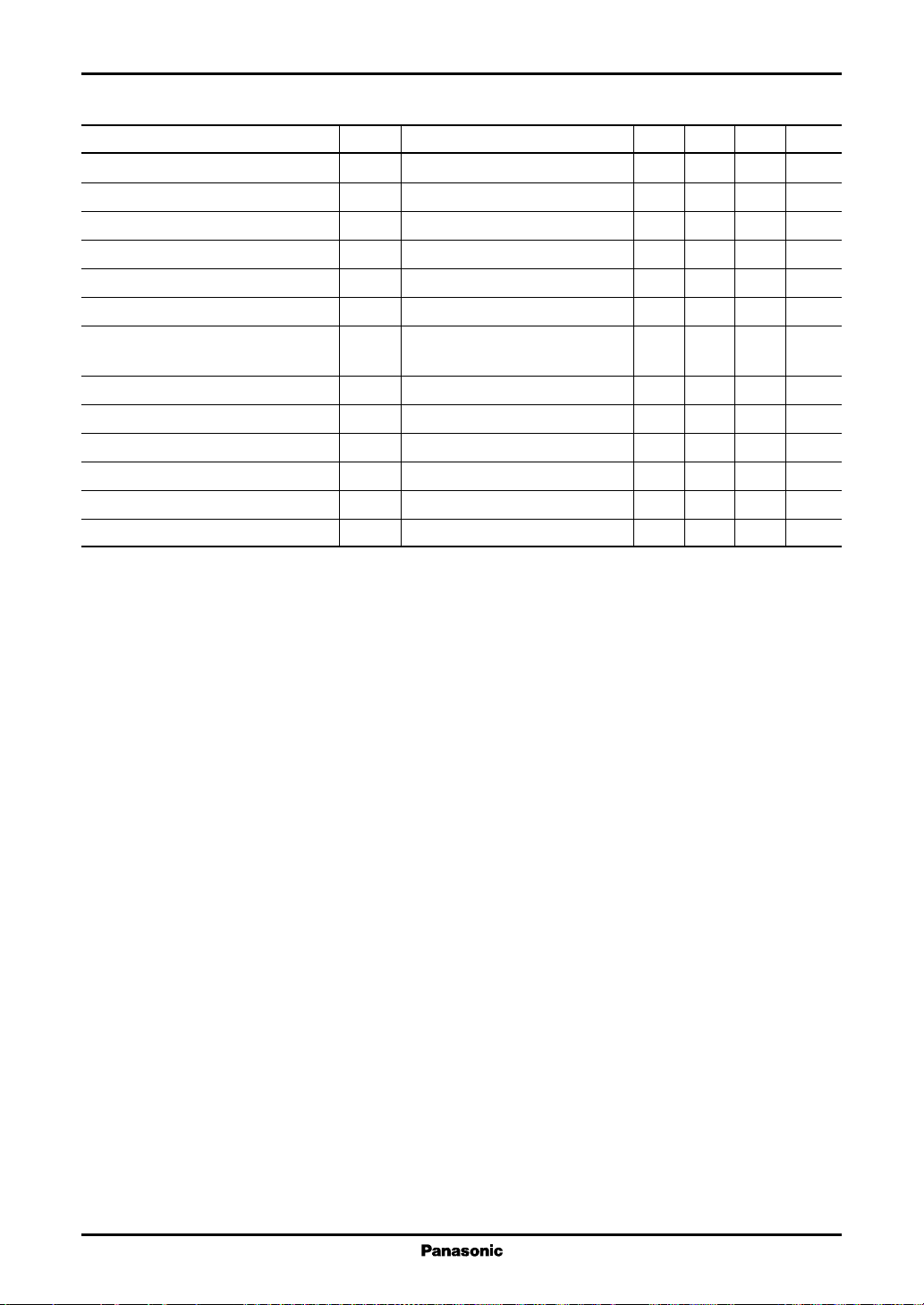
■ Electrical Characteristics at VCC = 19 V, f = 1 kHz, RL = 8 Ω, Ta = 25 °C
Parameter Symbol Conditions Min Typ Max Unit
Quiescent current I
1
Output end noise voltage
*
V
Voltage gain G
Total harmonic distortion THD VIN = 57 mV 0.2 0.4 %
Maximum Output Power P
Maximum Output power P
1
Ripple rejection ratio
*
Channel balance CB VIN = 57 mV −1.0 0 1.0 dB
Muting Ratio MR VIN = 57 mV 70 80 dB
Muting control voltage V
Standby control voltage 'on' V
Standby control voltage 'off' V
STD-ON
STD-OFF
Channel crosstalk CT VIN = 57 mV, Rg = 10 kΩ 50 60 dB
Note) *1: For this measurement, use the 20 Hz to 20 kHz (12 dB/OCT) filter.
VIN = 0 mV 35 70 mA
CQ
No input, Rg = 10 kΩ0.22 0.4 mV
NO
VIN = 57 mV 32 34 36 dB
V
VCC = 22 V, THD = 10 % 5.6 7.0 W
O
VCC = 19 V, THD = 10 % 4.0 5.0 W
O
RR Vr = 1 V
rms
45 55 dB
fr = 120 Hz, Rg = 10 kΩ
MUTEVIN
= 57 mV, MR ≥ 70 dB 3.0 V
No input, ICC ≤ 0.1 mA 5.0 V
No input, ICC ≥ 17 mA 8.5 V
3
 Loading...