

Panasonic AN5270 Datasheet

ICs for Audio Common Use
AN5270
4.3 W × 1(8Ω) Power Amplifier with Volume Control and Tone Control
■ Overview
The AN5720 is an integrated circuit designed for 4.3 W(8
Ω) power amplifier with volume control and tone control.
■ Features
• DC volume control : 0 to 5 V
• DC tone control : 0 to 5 V
• 9-lead single-in-line plastic package with fin
■ Block Diagram
Pre
amp.
Volume
control
Tone
control
19.9±0.1
18.3±0.25
φ2.65±0.1
φ3.3±0.1
0.1±0.05
8.4±0.25
5.8±0.25
1.5±0.25
5.6±0.25
6.3 7.1
±0.3 ±0.25
9
8
7
6
5
4
15.0
3
2
1
HSIP009-P-0000
Unit : mm
3.75±0.25
±0.1
0.5
1.2
2.54
+0.1
–0.05
1.7±0.25
0.45
±0.25
1.7
±0.25
22.3±0.3
1
V
CC1
2
In
3
LF
4
Vol-ctl.
5
Tone-ctl.
6
RF
■ Pin Descriptions
Pin No. Pin Name
1V
2 Sound input
3 Low frequency input
4 Volume control
5 Tone control
6 Ripple filter
7 Ground
8 Sound output
9V
Note) Pins 2 and 4 are weaker in protection against positive surge than the other pins.
It is necessary to pay attention during application use.
CC1
CC2
7
GND
8
Out
9
CC2
V
1
AN5270 ICs for Audio Common Use
■ Absolute Maximum Ratings
Parameter Symbol Ratings Unit
Supply voltage V
V
Circuit voltage V
Supply current I
3, 4
Circuit current
Power dissipation
Operating ambient temperature
Storage temperature
Note) Do not apply a current or voltage from the external to the terminals that are not described above.
*1:Ta = 25 °C, excluding parameters regarding ambient temperature and storage temperature.
*2:Ta = 70 °C, the IC is mounted on PCB, without external heat sink.
*3: For circuit currents, '+' denotes current flowing into the IC, and '−' denotes current flowing out of the IC.
*4: As the output Pin8 does not have over current protection circuit incorporated,
*
2
*
1
*
1
*
therefore please take precaution not to short the output pin to either VCC or GND.
)14 V
CC1(V1-7
)26
CC2(V9-7
2-7
V
3-7
V
4-7
V
5-7
CC1
I
CC2
I
8
P
D
T
opr
T
stg
0 to V
9-7
0 to V
9-7
0 to V
1-7
0 to V
1-7
15 mA
2A
−1.7 to +1.7 A
PP
1.6 W
−20 to +70 °C
−55 to +150 °C
■ Recommended Operating Range
Parameter Symbol Range Unit
Operating supply voltage range V
CC1
V
CC2
11 to 13 V
15 to 24
2
ICs for Audio Common Use AN5270
■ Electrical Caracteristics at V
= 12 V, V
CC1
= 18 V, f = 1 kHz, Ta = 25 °C, RL = 8 Ω, Vol. = max.,
CC2
Tone = max.
Parameter Symbol Conditions Min Typ Max Unit
Quiescent current 1 I
Quiescent current 2 I
TOT1
TOT2
Output DC bias V
Voltage gain G
Total harmonic distortion THD VO = 1 V
Max. output power Pomax THD = 10 %, PO = V
Max. output attenuation Attmax V
Tone variable range ∆G
No input signal 7 10 13 mA
Measure V
CC1
current
No input signal 20 28 48 mA
Measure V
No input signal 7.2 8.3 9.4 V
ODC
CC2
current
Measure Pin8 DC
V
VO = 1 V
= 1.0 V
O
, GV = 20 log(VO / VIN) 283032dB
rms
, BPF : 400 Hz to 30 kHz 0.5 1.0 %
rms
, Vol. = max. → min. −69 −66 dB
rms
Attmax = 20 log [V
f = 10 kHz, fix VIN where 18 20 dB
TC
V
O(tone = max.)
= 1 V
Tone = max. → min.
∆GTC = 20 log [V
2
/ R
O
O(vol. = max.)
rms
O(tone = max.)
L
/ V
/ V
O(tone = min.)
O(vol. = min.)
4.0 4.3 W
]
]
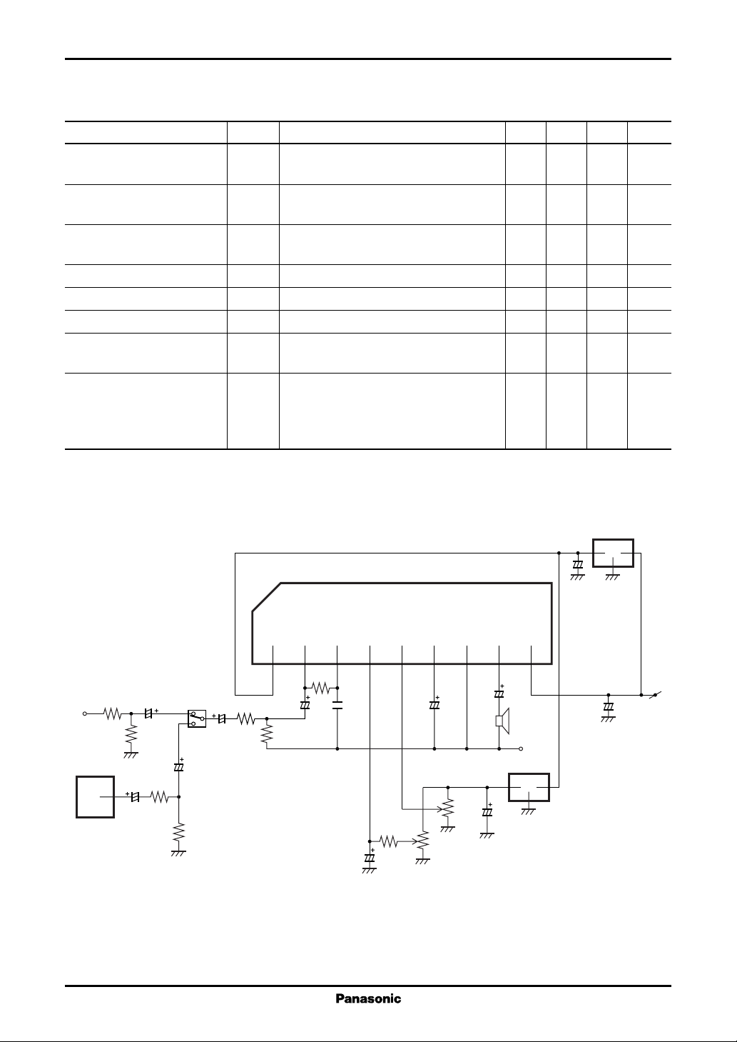
■ Application Circuit Example
AN5270
6
1In2LF3
5.1kΩ
CC1
100Ω
33µF
Ext
External
audio in
SIF-IC
Det.
out
33µF
Note) Design considerations for shock noise prevention. :
In the application of the IC, please adopt the above power supply configuration whenever possible.
Where this is not possible, then it is better to ensure that V
power-on shock noise. Similarly, please ensure that V
100kΩ
1kΩ
TV
AV
SW
33µF
9kΩ
33µF
24kΩ
V
3.3µF
30kΩ
4
5
Vol-ctl.
0.039
µF
22µF
CC2
Tone-ctl.
33kΩ
should start up first before the onset of V
CC1
declines faster than V
7
RF
GND
47µF
5V
10kΩ
VR
10kΩ
VR
, in order to prevent power-off shock noise.
CC1
Out 8
470
µF
8Ω
AN78M05
100µF
9
GND
12V
47µF
CC2
V
2200µF
, in order to prevent
CC2
AN78M12
18V
Power
supply
3
 Loading...