

Panasonic AN5195K-C Datasheet
ICs for TV
AN5195K-C
Single chip IC for PAL/NTSC color TV
2
(built-in I
■ Overview
The AN5195K-C is an IC in which all of the
PAL/NTSC system color television signal processing circuits are integrated on one chip. The rationalization of set production line can be realized by
the incorporation of I
C bus interface)
2
C bus interface.
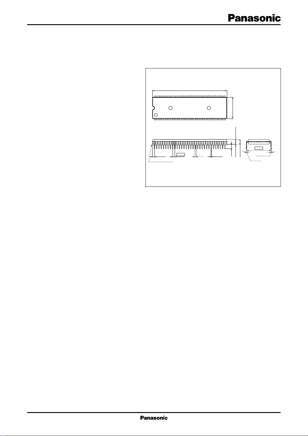
64 33
132
Unit: mm
58.4±0.3
17.0±0.2
■ Features
• Built-in video IF circuit, sound IF circuit, video
signal processing circuit, color signal processing
circuit, and sync. signal processing circuit
• Rationalization of set production line can be real-
ized by the incorporation of I
2
C bus interface
• Can be applied to PAL/NTSC/AV-NTSC/M-
NTSC system
• Package: 64-SDIP, supply voltage: 5 V, 9 V
■ Applications
• TV, TV-video combination
(1.641)
Seating plane
1.778
+0.1
– 0.05
0.5
(1.0)
SDIP064-P-0750B
(3.3)
3.85±0.2
5.2 max.
0.7 min.
19.05
0.25
0° to 15°
+0.1
– 0.05
1
AN5195K-C ICs for TV
■ Block Diagram
SIF3 in/ sharpness
Ext. audio in
SIF2 in
SIF1 in
IF AGC filter
Int. video1 in
SIF APC filter
Int. video2 in
VIF det. out
VIF APC1 filter
VIF VCO
Video out
Y-in
Sync. in
(VCJ)
V
CC3
C in/black expansion
GND(VCJ)
FBP in
V
CC2
AFC2 filter
AFC1 filter
Hor. VCO
X-ray protect
H-out
Ver. clamp
V-out
SECAM interface
−(B−Y) out
−(R−Y) out
S.C.P
−(B−Y) in
−(R−Y) in
33
34
35
36
37
38
39
40
41
42
43
44
45
46
47
48
49
50
51
52
53
54
55
56
57
58
59
60
61
62
63
64
*7-bit
VCO
Hor.
HBLK
reg.
Hor.
HVCO
Shut
down
out
Ver.
*6-bit
Saturation
APC1
sync. sep.
SCP
AFC1
Hor.
Ver.
SW
PN/S
*1-bit
G−Y
*2-bit
SIF SW
*1-bit
Video SW
*9-bit
CV
Ver.
AFC2
*3-bit
down
count
count down
B−Y
R−Y
Matrix
AFT Limiter
clamp
sync. sep.
BGP
*2-bit
(50 Hz
/60 Hz)
demod
+ / −
demod
SIF
detect
shift
Phase
*6-bit
Sharpness
Hor.
lock DET
50 Hz
/60 Hz
ident
Killer
RGB SW
LPF
Y
contrast
HVBLK
detect
VCO
*3-bit
Black
expansion
System
1H
Tint
LPF
SW
FF
B
De-
Level
adjust
Y
*1-bit
*6-bit
CW
clamp
emphasis
clamp
ACC
APC
generate
G
*1-bit
IF
VIF
amp.
clamp
Pre-amp.
AGC
detect
SW
DAC
1-bit
R
clamp
ASW
*6-bit
out
out
B
*Drive
G
R
*Drive
ACC
Chroma
2-bit
32
*1-bit
31
30
29
28
27
RF
26
AGC
25
IF
24
amp.
23
22
21
C bus
2
I
interface
20
19
18
17
7-bit
*Cut off
8-bit
16
*Cut off
8-bit
15
14
7-bit
*Cut off
8-bit
13
12
Contrast
11
(*6-bit)
10
det.
VCO
50 Hz/60 Hz
SECAM det SW
*
7-bit
Brightness Killer
Decoupling
Ext. video in
AFT out
De-emphasis
Audio out
RF AGC
GND(VIF/SIF)
VIF2 in
VIF1 in
(VIF/SIF)
V
CC3
SCL
SDA
ACL
GND (RGB/DAC)
Hor. lock det.
B-out
G-out
R-out
V
(9 V)
CC1
B-in
G-in
R-in
in
Y
S
9
BL det.
8
Chroma VCO (3.58 MHz)
7
Chroma VCO (4.43 MHz)
6
APC filter
5
Killer out,50 Hz/60 Hz out
SECAM det. out
4
Killer filter
3
(B) clamp filter
2
(G) clamp filter
1
(R) clamp filter
2
ICs for TV AN5195K-C
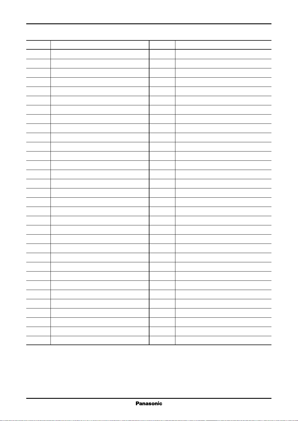
■ Pin Descriptions
Pin No. Description
1 (R) clamp
2 (G) clamp
3 (B) clamp
4 Killer filter
5
Killer out, 50 Hz/60 Hz out, SECAM det. out
6 Chroma APC filter
7 Chroma VCO (4.43 MHz)
8 Chroma VCO (3.58 MHz)
9 Black level det.
10 YS input
11 External R input
12 External G input
13 External B input
14 V
CC1
15 R output
16 G output
17 B output
18 Hor. lock detect
19 GND (RGB/I2C/DAC)
20 ACL
21 SDA
22 SCL
23 V
CC3-1
(VIF/SIF)
24 VIF1 input
25 VIF2 input
26 GND (VIF/SIF)
27 RF AGC output
28 Audio output
29 De-emphasis
30 AFT output
31 External video input
32 DC decoupling filter
Pin No. Description
33 SIF3 input/ sharpness
34 External audio input
35 SIF2 input
36 SIF1 input
37 IF AGC filter
38 Internal video1 input
39 SIF APC filter
40 Internal video2 input
41 VIF detect output
42 VIF APC1 filter
43 VIF VCO (fP/2)
44 Video output
45 Y input
46 HV sync. input
47 V
(chroma/jungle/DAC)
CC3-2
48 Chroma input/black expansion start
49 GND (video/chroma/jungle)
50 FBP input
51 V
(hor. stability supply)
CC2
52 AFC2 filter
53 AFC1 filter
54 Hor. VCO (32 fH)
55 X-ray protection input
56 Hor. pulse output
57 Ver. sync. clamp
58 Ver. pulse output
59 SECAM interface
60 −(B−Y) output
61 −(R−Y) output
62 Sandcastle pulse output
63 −(B−Y) input
64 −(R−Y) input
3
AN5195K-C ICs for TV
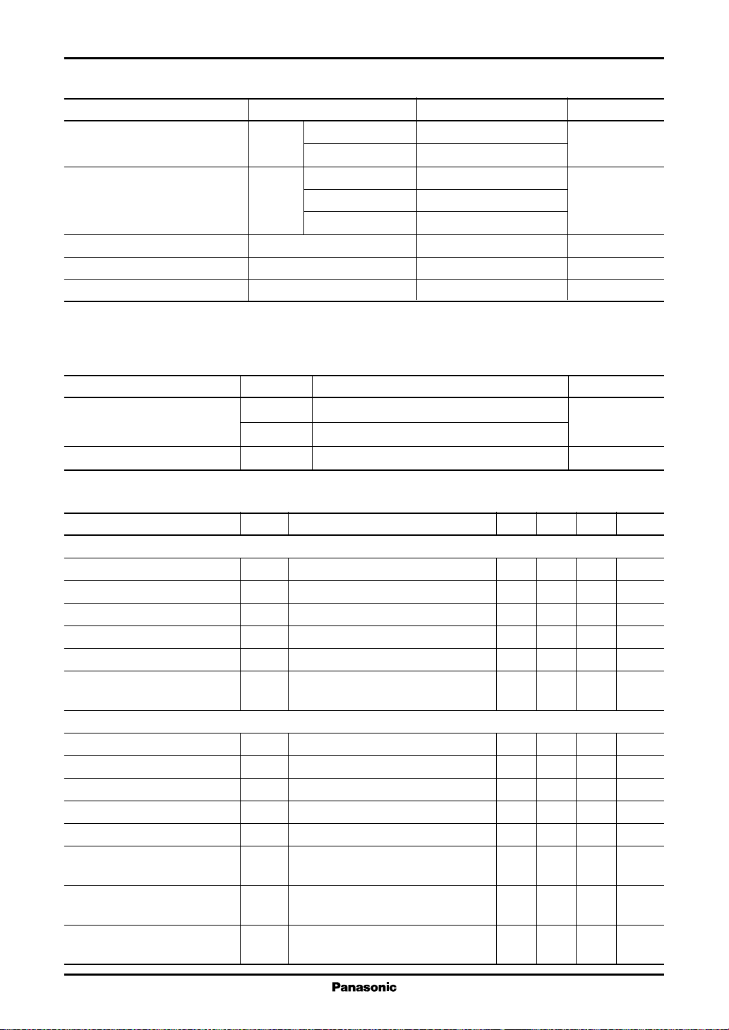
■ Absolute Maximum Ratings
Parameter Symbol Rating Unit
Supply voltage V
Supply current I
2
Power dissipation
*
Operating ambient temperature
1
Storage temperature
Note)*1 : Except fot the operating ambient temperature and storage temperature, all ratings are for Ta = 25°C.
2 : The power dissipation shown is the value for Ta = 70°C.
*
*
CC
CC
1
*
■ Recommended Operating Range
Parameter Symbol Range Unit
V
(14) 10.5 V
CC1
V
(23, 47) 6.0
CC3
I
14
I
23+47
I
51
P
D
T
opr
T
stg
67 mA
126
27
1,480 mW
−20 to + 70 °C
−55 to + 150 °C
Supply voltage V
Supply current I
CC1
V
CC3
51
■ Electrical Characteristics at Ta = 25°C
Parameter Symbol Conditions Min Typ Max Unit
Power supply
Supply current 1 I
Supply current 2 I
Supply current 3 I
Stabilized power supply voltage V
Stabilized power supply current I
Stabilized power supply R
input resistance at I51 = 10 mA and 25 mA
VIF circuit Typical input: fP = 38.9 MHz, VIN = 90 dBµ
Video detection output (typ.) V
Video detection output (max.) V
Video detection output (min.) V
Video detection output f characteristics
POmax
POmin
f
Sync. peak value voltage V
APC pull-in range (H) f
APC pull-in range (L) f
PPH
PPL
RF AGC delay point adjusting ∆V
range
Current at V14 = 9 V 394857mA
14
Current at V23 = 5 V 7 10 13 mA
23
Current at V47 = 5 V 496377mA
47
Voltage at I51 = 15 mA 5.8 6.5 7.2 V
51
Current at V51 = 5 V 2 5 7 mA
51
DC measurement, gradient 1 5 10 Ω
51
Modulation m = 87.5%, data 0B = 44 1.7 2.1 2.5 V[p-p]
PO
0B = 74 1.9 2.6 3.3 V[p-p]
0B = 04 1.1 1.6 2.1 V[p-p]
Frequency to become −3 dB for 1 MHz
PC
Sync. peak voltage at V[p-0] measurement
SP
High band side pull-in range 1.0 2.0 MHz
(difference from fP = 38.9 MHz)
Low band side pull-in range −2.0 −1.0 MHz
(difference from fP = 38.9 MHz)
Delay point (input to become 75 95 dBµ
RFDP
V
= approx. 6.5 V) at data 0A = 00 to 3F
27
8.1 to 9.9 V
4.5 to 5.5
10 to 25 mA
5.5 8 12 MHz
1.6 2.0 2.4 V
4
ICs for TV AN5195K-C
■ Electrical Characteristics at Ta = 25°C (continued)
Parameter Symbol Conditions Min Typ Max Unit
VIF circuit (continued) Typical input: fP = 38.9 MHz, VIN = 90 dBµ
VCO free-running frequency ∆f
RF AGC maximum sink current IRF
RF AGC minimum sink current IRF
AFT discrimination sensitivity µ
AFT center voltage V
AFT maximum output voltage V
AFT minimum output voltage V
AFTmaxV30
AFTminV30
Detection output resistance R
SIF circuit Typical input: fS = 6.0 MHz, fM = 400 Hz, VIN = 90 dBµ
Audio detection output V
SOP36
(PAL, SIF1) 0B−D3 = 0
Audio detection output V
SOP35
(PAL, SIF2) 0B−D3 = 0
Audio detection output V
SOP33
(PAL,SIF3) 0B−D3 = 0
Audio detection output NTSC/PAL
R
SN/P
Audio detection output linearity ∆V
SIF pull-in range f
NTSC (4.5 MHz)
SIF pull-in range f
NTSC (4.5 MHz)
SIF pull-in range f
PAL (5.5 MHz)
SIF pull-in range f
PAL (5.5 MHz)
SIF pull-in range f
PAL (6.0 MHz)
SIF pull-in range f
PAL (6.0 MHz)
SIF pull-in range f
PAL (6.5 MHz)
SIF pull-in range f
PAL (6.5 MHz)
SNH
(4.5 MHz)
SNL
(4.5 MHz)
SPH
(5.5 MHz)
SPL
(5.5 MHz)
SPH
(6.0 MHz)
SPL
(6.0 MHz)
SPH
(6.5 MHz)
SPL
(6.5 MHz)
De-emphasis pin R
output resistance (PAL)
De-emphasis pin R
output resistance (NTSC)
Dispersion without input VIN, −1.2 0 1.2 MHz
P
V37 (IF AGC) = 0 V(measurement of
difference from 38.9 MHz)
Maximum current IC can sink when pin 27 is low
max
Leakage current of IC, when pin 27 is high
min
∆f = ±25 kHz 40 57 75 mV/kHz
AFT
V30 without input V
AFT
IN
1.5 3.0 mA
−50 0 50 µA
4.0 4.5 5.0 V
at f = fP −500 kHz 7.8 8.1 8.7 V
at f = fP +500 kHz 0.3 0.8 1.0 V
DC measurement IO = − 0.4 mA to −1.0 mA
O41
70 120 170 Ω
∆f = ±50 kHz 0.90 1.15 1.40 V[rms]
∆f = ±50 kHz 0.90 1.15 1.40 V[rms]
∆f = ±50 kHz 0.90 1.15 1.40 V[rms]
∆f = ±25 kHz, 0B−D3 = 1, ratio to PAL (V
Ratio between fS = 5.5 MHz −30 3 dB
SOP
)
−2.5 − 0.5 1.5 dB
SOP36
and 6.0 MHz, and 6.5 MHz
Pull-in range of high frequency side 4.8 5.0 MHz
Pull-in range of low frequency side 4.0 4.2 MHz
Pull-in range of high frequency side 5.8 6.0 MHz
Pull-in range of low frequency side 5.0 5.2 MHz
Pull-in range of high frequency side 6.3 6.5 MHz
Pull-in range of low frequency side 5.5 5.7 MHz
Pull-in range of high frequency side 6.8 7.0 MHz
Pull-in range of low frequency side 6.0 6.2 MHz
Impedance of pin 29 at PAL 32 40 48 kΩ
29P
Impedance of pin 29 at NTSC 48 60 72 kΩ
29N
5
AN5195K-C ICs for TV
■ Electrical Characteristics at Ta = 25°C (continued)
Parameter Symbol Conditions Min Typ Max Unit
AV SW circuit
Video SW voltage gain G
Video SW f characteristics f
Video SW external input pin voltage
Video SW external output DC voltage
Video SW external input resistance
VSW
VSW
V
V
R
Video SW output resistance R
Video SW internal clamp pin voltage
Video SW internal output DC voltage
Audio SW voltage gain G
V
38,40
V
ASW
Audio SW input pin voltage V
Audio SW output DC voltage V
Audio SW input resistance R
Audio SW output resistance R
Video signal processing circuit Typical input: 0.6 V[p-p] (VWB = 0.42 V[p-p] stair-step), at G-out
Video output (typ.) V
Video output (max.) V
Video output (min.) V
Contrast variable range Y
YOmax
YOmin
Cmax/min
Video frequency characteristics f
Picture quality variable range Y
Smax/minV33
Pedestal level (typ.) V
Pedestal level variable width ∆V
Brightness control sensitivity ∆V
Video input clamp voltage V
YCLP
ACL sensitivity AC L
Blanking off threshold voltage V
Blanking level V
1
Service SW threshold voltage
*
DC restoration ratio T
Video input clamp current I
Note)*1:
Take great care for not to become V20 < 0.9 V at set design so that the pin 20 is combined use for service SW when it is used as the ACL
YCLP
f = 1MHz, VIN = V[p-p] 5.7 6.7 7.7 dB
Frequency to become −3 dB 8 10 MHz
from f = 1 MHz, VIN = 0.714 V[0-p]
DC measurement 1.7 2.0 2.3 V
31
DC measurement, 03−D7 = 1, 0B−D7 = 1
44E
DC measurement 44 56 68 kΩ
I31
DC measurement, IO = − 0.6 mA to −1.0 mA
O44
4.2 4.8 5.4 V
100 140 180 Ω
DC measurement, IIN = −1.0 mA 1. 3 1.6 1.9 V
DC measurement 3.7 4.3 4.9 V
44I
Data 03−D7 = 1, 0B−D7 = 1 −10 1 dB
(external input) f = 400 Hz, VIN = 1 V[p-p]
DC measurement 3.7 4.2 4.7 V
34
DC measurement 3.7 4.2 4.7 V
28
DC measurement 55 65 75 kΩ
I34
DC measurement 200 400 600 Ω
O28
Data 03 = 20 (typ.) (contrast) 1.9 2.4 2.9 V[0-p]
YO
Data 03 = 3F (max.) 4.1 5.0 5.9 V[0-p]
Data 03 = 00 (min.) 0.15 0.50 1.00 V[0-p]
03 = 3F 15 20 25 dB
03 = 00
Pin 33 = 5 V (sharpness), frequency 5.5 6.0 MHz
YC
to become −3 dB from f = 0.2 MHz
= 7 V
V33 = 5 V
Data 02 = 40 (typ.) (brightness) 2.0 2.5 3.0 V
PED
Difference between data 02 = 00 and 7F
PED
Average amount of change 14 20 26 mV/
BRT
, f = 3.8 MHz
91317dB
2.0 2.6 3.2 V
at data 02 = 30 and 50 per 1 step Step
Clamp voltage of pin 45 3.2 3 .7 4.2 V
Change of Y-out, when V20 = 3.0 V → 3.5 V
DC voltage of blanking pulse 1.0 1.5 V
YBL
Stop voltage of vertical output, 0.3 V
STH
2.4 3.0 3.6 V/V
when lowering pin 20 (ACL) voltage
APL 10% to 90% 90 1 0 0 110 %
DC
∆AC − ∆DC
TDC =
∆AC
DC measurement: IC inside sink current
× 100
81318µA
.
6
ICs for TV AN5195K-C
■ Electrical Characteristics at Ta = 25°C (continued)
Parameter Symbol Conditions Min Typ Max Unit
Video signal processing circuit (continued) Typical input: 0.6 V[p-p] (VWB = 0.42 V[p-p] stair-step), at G-out
Pedestal difference voltage ∆V
Brightness voltage tracking ∆T
Video voltage gain relative ratio ∆G
Video voltage gain tracking ∆T
Chroma signal processing circuit Burst 150 mV[p-p] (PAL), reference is B-out
Color-difference output (typ.) V
Color-difference output (max.) V
Color-difference output (min.) V
Contrast variable range C
COmax
COmin
Cmax/min
ACC characteristics 1 ACC1 Burst 150 mV[p-p] → 300 mV[p-p] 0.9 1.0 1.2 Times
ACC characteristics 2 ACC2 Burst 150 mV[p-p] → 30 mV[p-p] 0.8 1.0 1. 2 Times
NTSC tint center ∆θ
NTSC tint variable range 1 ∆θ
NTSC tint variable range 2 ∆θ
Color-difference output ratio (R)
Color-difference output ratio (G)
Color-difference output angle (R)
Color-difference output angle (G)
PAL color killer tolerance V
NTSC color killer tolerance V
APC pull-in range (H) f
APC pull-in range (L) f
R/B Input: Rainbow for both PAL/NTSC 0.46 0.56 0.66 Times
G/B Input: Rainbow for both PAL/NTSC 0.28 0.34 0.40 Times
∠R Input: Rainbow for both PAL/NTSC 7 8 90 102 deg
∠G Input: Rainbow for both PAL/NTSC 22 4 236 248 deg
KILLP
KILLN
CPH
CPL
Color killer detection V
output voltage (color)
Color killer detection V
KBW
output voltage (B&W)
Demodulation output −(B−Y) V
Demodulation output −(R−Y) V
Demodulation output angle ∠(B−Y)
Demodulation output angle ∠(R−Y)
CW output level (4.43 MHz) V
∠R
∠R
CWP
Difference voltage of R,G,B-out pedestal
IPL
R,G,B-out fluctuation level ratio of 0.9 1.0 1.1 Times
BL
− 0.2 0 0.2 V
data 02 (brightness) = 20 to 60
Output ratio of R,B-out against G-out 0.8 1.0 1.2 Times
YC
Gain ratio of R,G,B-out at data 03 0.9 1.0 1.1 Times/
CONT
(contrast) = 10 to 30 Times
Input: Color bar data 2.9 3.7 4.5 V[p-p]
CO
00 = 20 (typ.), 03 = 20 (typ.)
Data 00 = 3F, amplitude of one side, 03 = 20
2.6 3.3 V[0-p]
Data 00 = 00, 03 = 20 10 0 mV[p-p]
03 = 3F
03 = 00
Difference from data 01 = 20 (tint), −7 0 7 Step
C
, 00 = 20
15 20 25 dB
when adjusted at tint center
Input: Rainbow, data 01 = 3F 30 50 65 deg
1
Input: Rainbow, data 01 = 00 −65 −50 −30 deg
2
0 dB = 150 mV[p-p] −57 −44 −34 dB
0 dB = 150 mV[p-p] −57 −44 −34 dB
For both PAL/NTSC 450 700 Hz
For both PAL/NTSC −700 −450 Hz
V5, when chroma input 4.5 5.0 V
KC
Data 0A−D6 = 0, 0A−D7 = 1, killer out
V5, when chroma input 0 0.1 0.5 V
Data 0A−D6 = 0, 0A−D7 = 1, killer out
Input: Measurement at pin 60 5 5 5 695 83 5 mV[p-p]
DB
for both color bar PAL/NTSC
Input: Measurement at pin 61 4 3 0 540 65 0 mV[p-p]
DR
for both color bar PAL/NTSC
Phase shift of B−Y axis −6 0 6 deg
DB
Phase difference from B−Y axis 84 90 96 deg
DR
AC component, when VCO is set at 4.43 MHz
250 350 450 mV[p-p]
7
AN5195K-C ICs for TV
■ Electrical Characteristics at Ta = 25°C (continued)
Parameter Symbol Conditions Min Typ Max Unit
Chroma signal processing circuit (continued) Burst 150 mV[p-p] (PAL), reference is B-out
CW output level (3.58 MHz) V
CW output level period (SECAM)
SECAM discrimination current I
CWN
T
SECAM
SECAM discrimination output V
PAL/NTSC DC level V
59PN
SECAM DC level V
RGB processing circuit DAC data are typical
Drive adjustment range G
Cut-off adjustment range V
YS threshold voltage V
YS threshold voltage V
External RGB pedestal difference voltage
CUTOFF
YSON
YSOFF
∆V
Internal and external pedestal ∆V
difference voltage
External RGB output voltage V
External RGB output difference voltage
External RGB contrast variable E
ERGB
∆V
Cmax/min
range 03 = 00
External RGB frequency characteristics
f
RGBC
Internal and external RGB V
output voltage ratio input, contrast 03 = 20 (typ.)
Synchronizing signal processing circuit
Horizontal free-running f
oscillation frequency
Horizontal output pulse duty cycle
τ
Horizontal pull-in range f
PAL vertical free-running f
VO-P
oscillation frequency
NTSC vertical free-running f
VO-N
oscillation frequency
Vertical output pulse width τ
PAL vertical pull-in range f
NTSC vertical pull-in range f
VP-P
VP-N
Horizontal output voltage (H) V
Horizontal output voltage (L) V
AC component, when VCO is set at 3.58 MHz
CW output period at SECAM and PAL
CW
50 mV[p-p]
1.31 1.41 1.51 ms
Minimum value for taking out current 50 100 150 µA
from pin 59 and discriminating as SECAM
V5 data, when SECAM signal inputted
SE
4.5 5.0 V
0A−D6 = 1, 0A−D7 = 0, SECAM det. out
V59 DC level at PAL/NTSC 0.8 1.3 1.65 V
V59 DC level at SECAM 4.1 4 . 6 5.1 V
59S
AC change amount of R, B-out, 5 6 7 dB
DV
when drive adjustment max. and min.
DC change amount of R,G,B-out, 2.1 2.4 2.7 V
when cutoff adjustment max. and min.
Minimum DC voltage, when YS turns on
Maximum DC voltage, when YS turns off
YS = 5 V −200 0 200 mV
EPL
Internal-external 200 0 200 mV
PL/IE
Input 0.7 V[p-p], contrast 03 = 20 (typ.)
Output ratio of external R,G,B-out 0.8 1.0 1. 2 Times
ERGB
1.0 V
0.4 V
1.8 2.2 2.7 V[p-p]
03 = 3F 12 17 22 dB
Input 0.2 V[p-p] 8 10 MHz
External 0.7 V[p-p]/internal 0.6 V[p-p]
E/I
Without sync. signal input 15.33 15.63 15.93 kHz
HO
Upward going pulse duty cycle 31 37 43 %
HO
Difference from fH = 15.625 kHz ±500 ±650 Hz
HP
0.78 0.92 1.06 Times
Data 01−D7 = 1, 02−D7 = 0 485052 Hz
Forced 50 Hz mode, no sync. signal input
Data 01−D7 = 1, 02−D7 = 1 586062 Hz
Forced 60 Hz mode, no sync. signal input
For both PAL/NTSC 9 10 11 1/fH
VO
fH = 15.625 kHz, forced 50 Hz mode 46 54 Hz
fH = 15.75 kHz, forced 60 Hz mode 5 6 64 Hz
High-level DC voltage 2.9 3.2 3.5 V
56H
Low-level DC voltage 0.3 V
56L
8
 Loading...