

Panasonic AN5186FB Datasheet
ICs for TV
AN5186FB
VIF/SIF IC for car-TV
■ Overview
The AN5186FB is a VIF/SIF signal processing IC for
in-car television. The video and sound are completely
separated by the adoption of split carrier method. Also,
high performance and high function have been realized
by the incorporation of in-car circuits such as soft mute
and SD.
■ Features
• Split carrier method sound detection circuit
• Electric field detection and band detection type soft
mute and SD
• Multipath detection circuit
• VIF uses quasi-synchronous detection which is invul-
nerable to electric field fluctuation.
• Video output pin for diversity detection (no noise
inverter)
■ Applications
• In-car televisions
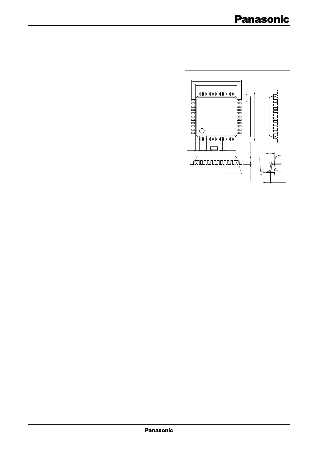
12.00±0.20
10.00±0.20
33 23
34
44
111
(1.00)
0.80
+0.10
0.35
–0.05
Seating plane
QFP044-P-1010C
(1.00)
22
12
12.00±0.20
10.00±0.20
1.95±0.20
–0.05
+0.10
0.15
0.10±0.10
Unit : mm
(1.00)
0° to 10°
0.50±0.20
1
AN5186FB ICs for TV
■ Block Diagram
RF AGC
delay
SIF in
SIF in
GND1
VIF in
VIF in
RF AGC
output (R)
V
REG
AFT out
34
35
36
37
38
39
40
41
42
43
44
33
OSC
Regulator
Mixer
IF
AGC
VIF
amp.
RF
AGC
32
Regulator
Carrier
amp.
31
V
CC3
30
Buffer
amp.
Detector
29
AFT
SD out
SD
detector
GND3
28
27
Video
amp.2
1st
limiter
V cont.
detector
V cont.
DC amp.
Noise
inverter
Video
amp.1
26
25
REF
V
24
Regulator
Multipath
23
2nd
limiter
Mute
amp.
Quad
detector
AFC
amp.
band
detector
detector
22
GND2
21
20
19
V
REF
18
V
CC
17
16
V
CC2
15
Multipath out
14
13
Multipath in
12
V cont. out1
1
2
3
CC1
V
■ Pin Descriptions
Pin No. Description
1V
2 VIF detection coil 1
3 VIF detection coil 2
4 SSC
5 AFT detection coil
6 AMDC adjustment
7 Video output 2
8 Video output 1
9 SMTC1
2
CC1
4
5
6
7
8
9
10
11
REF
V
Video out2
Video out1
Audio out
Pin No. Description
10 Audio output
11 SMTC2
12 S meter output
13 AMDC input
14 AMDC detection
15 AMDC output
16 AFC output
17 V
CC2
18 SIF detection coil
ICs for TV AN5186FB
■ Pin Descriptions (continued)
Pin No. Description
Pin No. Description
19 SMA1
20 SMA2
21 2nd limiter input
22 GND2
23 1st limiter output
24 SIF reference voltage
25 V cont. adjustment
26 1st limiter bypass
27 1st limiter input
28 GND3
29 SD output
30 Mixer output
31 V
CC3
32 OSC1
33 OSC2
34 RF AGC delay adjustment
35 IF AGC output
36 IF AGC input
37 SIF input 1
38 SIF input 2
39 GND 1
40 VIF input 1
41 VIF input 2
42 RF AGC output
43 VIF reference voltage
44 AFT output
■ Absolute Maximum Ratings
Parameter Symbol Rating Unit
Supply voltage V
Supply current I
2
Power dissipation
Operating ambient temperature
Storage temperature
Note)*1: Ta = 25°C except power dissipation, operating ambient temperature and storage temperature.
2: The power dissipation is for the IC only when Ta = 85°C in free air.
*
*
1
*
1
*
CC
CC
P
D
T
opr
T
stg
V
, V
, I
CC2
CC2
, V
, I
CC3
CC3
CC1
I
CC1
425 mW
−30 to +85 °C
−55 to +150 °C
10.2 V
80 mA
■ Recommended Operating Range
Parameter Symbol Range Unit
Supply voltage V
CC1
, V
CC2
, V
CC3
7.2 to 10.0 V
3
AN5186FB ICs for TV
■ Electrical Characteristics at Ta = 25°C, V
CC1
= V
CC2
= V
CC3
= 8.0 V
Parameter Symbol Conditions Min Typ Max Unit
VIF block
Video detection output 1 V
Video detection output 2 V
Sync. peak value voltage 1 V
Sync. peak value voltage 2 V
Video frequency characteristic f
RF AGC operating sensitivity G
Video: 10 stairs − Y, m = 87.5% 1.7 2.0 2.3 V[p-p]
O8
Video: 10 stairs − Y, m = 87.5% 1.7 2.0 2.3 V[p-p]
O7
P8
P7
Output −3dB frequency for 1 MHz 6 8 MHz
C
Input level difference to become 1.0 3.0 dB
RF
2.7 3.1 3.5 V
2.7 3.1 3.5 V
V42 = 1.5 → 7 V
RF AGC maximum sink current I
RF AGC minimum sink current I
AGCmaxV34
AGCminV34
AFT detection sensitivity µ
AFT maximum output voltage V
AFT minimum output voltage V
Video output resistance 1 R
Video output resistance 2 R
AFT
AFTmax
AFTmin
O8
O7
= 2.5 V, V36 = 2 V 2.2 2.9 3.6 mA
= 2.5 V, V36 = 3 V −20 2 µA
∆f = ±25 kHz 13 20 27 mV/kHz
f = fP − 500 kHz 4.2 4.7 5.0 V
f = fP + 500 kHz 0 0.3 0.8 V
V36 = 0 V 20 50 120 Ω
V36 = 0 V 20 50 120 Ω
SIF block/mixer block
S meter gradient 1 ∆VS1f = 10.7 MHz 1.3 1.7 2.1 V
S meter gradient 2 ∆VS2f = 10.7 MHz 1.45 1.85 2.25 V
V
Audio detection output V
OS
= 70 dBµ, f = 10.7 MHz, 125 160 19 5 mV[rms]
IN27
fM = 1 kHz, ∆f = ±25 kHz
Mix. conversion gain V
Audio output resistance R
S meter output resistance (pin 12)
Circuit current I
CG
O10
R
O12
CC
No modulation, V
V
, V
CC2
, V
CC3
CC1
= 70 dBµ 24 30 dB
IN37
260 380 500 Ω
60 160 260 Ω
= 8.0 V 51 63 75 mA
• Design reference data
Note) The characteristic values below are theoretical values for designing and not guaranteed.
Parameter Symbol Conditions Min Typ Max Unit
VIF block
VIF input sensitivity V
VIF maximum allowable input V
Input level to become VO8 = −3 dB 42 49 dBµ
VS
Input level to become VO8 = +1 dB 103 108 dBµ
Vmax
Video S/N S/NVBPF: 10k to 4M 50 56 dB
Differential gain DG Video: 10 − stairs 0 4 8 %
Differential phase DP Video: 10 − stairs 0 4 8 %
Intermodulation IM P/C = 2 dB, P/S = 12 dB 30 36 dB
Black noise detection level ∆VBN
Black noise clamp level ∆V
Difference from sync. peak value voltage
Difference from sync. peak value voltage
BNC
− 0.85 V
0.6 V
4
ICs for TV AN5186FB
■ Electrical Characteristics at Ta = 25°C, V
CC1
= V
CC2
= V
= 8.0 V (continued)
CC3
• Design reference data (continued)
Note) The characteristic values below are theoretical values for designing and not guaranteed.
Parameter Symbol Conditions Min Typ Max Unit
VIF block (continued)
AFT defeat SW operating voltage
VIF input resistance R
VIF input capacitance C
VIF reference voltage V
V
AFTSW
0.4 0.8 V
f = 58.75 MHz 1.8 kΩ
140
f = 58.75 MHz 3.2 pF
140
REG
5.0 V
SIF/mixer block
S meter voltage 1 V
S meter voltage 2 V
S meter voltage 3 V
S meter voltage 4 V
AFC offset voltage V
Limiting sensitivity V
V
S1
IN27
V
S2
IN27
V
S3
IN27
V
S4
IN27
AFCVIN27
LIMV0
= 0 dB, input for 3 dB down 32 38 dBµ
= without input 0.05 0.5 1.1 V
= 40 dBµ 1.0 1.7 2.4 V
= 70 dBµ 2.3 3.4 4.5 V
= 100 dBµ 3.9 5.2 6.5 V
= without input − 0.1 0 0. 1 V
SD sensitivity SDS Input when SD output becomes 4.5 V 38 dBµ
or more at V4 = 2 V
SD bandwidth SDW Bandwidth when SD output becomes 140 kHz
4.5 V or more at V4 = 2 V
SIF input resistance R
SIF input capacitance R
Mixer output resistance R
S/N sensitivity N
f = 54.25 MHz 2.7 kΩ
I37
f = 54.25 MHz 3.2 pF
C37
f = 10.7 MHz 300 Ω
O30
OUTVIN37
= 22 dBµ no modulation, 22 30 dB
however, S is the output when 1 kHz
100% modulation.
Audio S/N S/NA 60 65 dB
AM rejection ratio AMR V
= 70 dBµ, AM = 30% 48 54 dB
IN27
Total harmonic distortion THD fM = 1 kHz, ∆f = ±25 kHz 0 0.2 1.0 %
Soft mute attenuation ∆Mute 50 dB
Multipath detection ∆VMPf = 100 kHz, V
SIF reference voltage V
REF
= 70 dBµ, 110 dBµ 1.5 V
IN13
4.1 V
5
 Loading...