

Panasonic AN5165K Datasheet
ICs for TV
AN5165K
A Single Chip IC for NTSC Color-TV
■ Overview
The AN5165K is an IC in which all of the NTSC
system color television signal processing circuits are integrated on a single chip. The rationalization of set production line can be realized by this IC incorporating I
2
bus interface.
■ Features
• Built-in video IF circuit, sound IF circuit, video signal
processing circuit, color signal processing circuit, deflection correction circuit and sync. signal processing
circuit
• Built-in I
2
C bus interface
■ Applications
• TVs
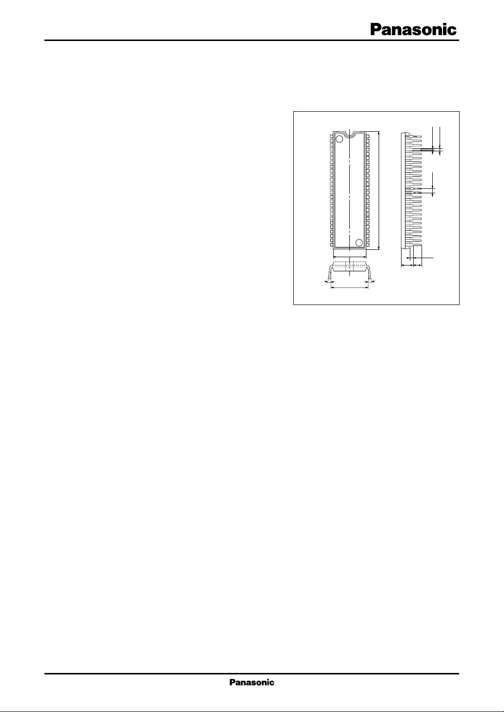
Unit: mm
1
52
0.5±0.1
1.0±0.25
C
1.778
47.7±0.3
26 27
3° to 15°
13.7±0.3
(15.24)
3° to 15°
SDIP052-P-0600A
3.85±0.3 (3.3)
(0.7)
1
AN5165K ICs for T V
■ Block Diagram
26
Drive
SW
M
&Y
S
Y
VCO
25
24
23
22
21
20
19
18
17
16
15
14
13
12
11
10
9
8
7
Cut Off B SW
Cut Off R SW
6
5
4
3
2
1
Decoupling
Ext.Video
Audio Out
APC
RF AGC Out
GND (IF)
IF 5 V
9 V
BLK In (SCP)
SCL
SDA
ACL/NECK
GND (RGB)
Lock DET
B
G
R
V/C/J 9 V
B In
G In
R In
Y
S&YM
APC
Chroma VCO
Ext.Audio
SIF In
IF AGC
Video Out
AFT Out
Int.V
DET Out
APC
VCO1
VCO2
IF 9 V
BLDET
V Sync. Y In
V Clamp
H Sync.
V/C/J/5 V
C In
VCJ GND
FBP In
6.3 V
AFC1
HOSC
X-ray
H Out
CW Out
V Out1
27
5-bit
DEMP
AFT
DAC
9-bit
IF
DAC
DET
VOL
7-bit
ASW
RF
AGC
DAC
VIF
Amp.
28
29
30
31
DC
SIF
VSW
SW
V SW
VA
RAMP
SW
IF
PLL
AGC
32
4-bit
33
34
DAC
VAMP
VCO
CTRL
35
36
VCO
PT
NI
APC
37
B.G.P
CCP (Hosc4)
H Out2
VBLK
Trig1
SW
to Video
Trig2
RGB
L.P.F.
3-bit
A Trig
Sharpness
Y.N.R
DAC
to Chroma
H Center
P.EQP
DACSW
5-bit
DAC
6-bit
7-bit
DAC
On/Off SW
B.P.F.1
SW
ACC1
ACC DET
Killer Off SW
Y Contrast
SW
ABL SW
L.P.F.
B.P.F.2
BPF SW
ACC2
Killer
SW
DAC
Bright
Y Clamp
Contrast
CW Out
8-bit
Black
DC
7-bit
DAC
Color
γ
Expamsion
C Filter
7-bit
Drive
8-bit
Cut Off
DEM
APC
7-bit
DAC
Tint
γ On/Off SW
SW
3-bit
DAC
RGB Limit
Cut off
DACDAC
Gain Control
38
39
CV Clamp
DL Trap
40
41
42
Hor.
43
Sync. Sep.
44
to Video
45
Ver.
Sync. Sep.
HBLK
Lock DET
46
HBLK
47
Hosc1
2fH
Ver.
H Pluse
CountDown
Hosc2
Hor.
AFC2
H Out1
CountDown
48
AFC1
HVCO
49
S.SW
SW
X-ray
Ver. Out
32fH
H.EQP
50
51
52
2
ICs for TV AN5165K
■ Pin Description
Pin No. Description
1 Chroma VCO (3.58 MHz)
2 Chroma APC Filter
3Y
& YM Input
S
4 External R Input
5 External G Input
6 External B Input
7V
9 V (VCJ)
CC1-1
8 R Output
9 G Output
10 B Output
11 Hor. Lock Detect
12 GND (RGB/I2C/ DAC)
13 ACL/NECK Protect
14 SDA
15 SCL
16 BLK Pulse Input/H
SYNC2
17 White Detect
18 V
5 V (VIF/SIF)
CC2-1
19 VIF Input (1)
20 VIF Input (2)
21 GND (VIF/SIF)
22 RF AGC Output
23 SIF APC Filter
24 Audio Output
25 External Video Input
26 DC Decoupling Filter
27 External Audio Input
Output
Pin No. Description
28 SIF Input/White Expand-Level
29 IF AGC Filter
30 Video Output
31 AFT Output
32 Internal Video Input
33 VIF Detect Output
34 VIF APC Filter
35 VIF VCO (1)
36 VIF VCO (2)
37 V
CC1-2
9 V
38 Black Detect
39 Y/Ver. Sync. Input
40 Ver. Sync. Clamp
41 Hor. Sync. Input
42 V
5 V (Chroma/jungle/DAC)
CC2-2
43 Chroma Input/Black Expansion Start
44 GND (Video/Chroma/Jungle)
45 FBP Input
46 V
CC3
6.2 V
47 AFC1 Filter
48 Hor. VCO (32 fH)
49 X-ray Protection Input
50 Hor. Pulse Output
51 CW Output/Spot KILLER Off Input/
X-ray Protection Output
52 Ver. Pulse Output
■ Absolute Maximum Ratings
Parameter Symbol Rating Unit
Supply voltage V
Supply current I
CC
CC
V
(7·37) 10.5 V
CC1
V
(18·42) 6.0
CC2
V
(46) 6.5
CC3
I
7+37
I
18+42
I
46
117 mA
68
6.3
3
AN5165K ICs for T V
■ Absolute Maximum Ratings (continued)
Parameter Symbol Rating Unit
2
Power dissipation
Operating ambient temperature
Storage temperature
Note)*1: Except for the operating ambient temperature and storage temperature, all ratings are for Ta = 25°C.
2: The power dissipation shown is the value for Ta = 70°C
*
■ Recommended Operating Range
Supply voltage V
■ Electrical Characteristics at Ta = 25°C
Power supply
*
1
*
1
*
P
D
T
opr
T
stg
1 481 mW
−20 to +70 °C
−55 to +150 °C
Parameter Symbol Range Unit
CC1
V
CC2
V
CC3
8.1 to 9.9 V
4.5 to 5.5
6.05 to 6.35
Parameter Symbol Conditions Min Ty p Max Unit
Supply current 1 I
7+I37
Current at V7 = 9 V, current at 68 85 100.5 mA
V37 = 9 V
Supply current 2 I
18+I42
Current at V18 = 5 V, current at 38 48 57 mA
V42 = 5 V
Supply current 3 I
Supply current 4 I
Current, when V46 = 6.2 V 2 5 6 mA
46
Current at V46 = 6.2 V. However 5 7 9 mA
46
all other power supplies are off state
VIF circuit (Typical input fP = 45.75 MHz, VIN = 90 dBµ)
Video detection output (typ.) V
Modulation factor m = 87.5% 1.75 2.1 2.5 V[p-p]
PO
Data 0D = 88
Video detection output (max.) V
Video detection output (min.) V
Video detection output f characteristics
Synchronous peak value voltage V
APC pull-in range (Hu) f
POmax
PPHU
Data 0D = F8 2.15 2.6 3.3 V[p-p]
Data 0D = 08 1.1 1.6 2.0 V[p-p]
POmin
f
Frequency of output −3 dB for 1 MHz 5.5 8 12 MHz
PC
Voltage in VPO measurement 1.6 2.0 2.4 V
SP
High band side pull-in range 1.0 1.5 MHz
(Difference from fP = 45.75 MHz)
APC pull-in range (Lu) f
PPLU
Low band side pull-in range −1.5 −1.0 MHz
(Difference from fP = 45.75 MHz)
RF AGC delay point adjustment DV
range (V
Input to become delay point 75 95 dBm
RFDP
= approx. 6.5 V), when Data
22
0C = 00 to 7F
RF AGC maximum sink current I
4
RFmax
Maximum current IC can sink when 1.5 3.0 mA
pin 22 is low
ICs for TV AN5165K
■ Electrical Characteristics at Ta = 25°C (continued)
Parameter Symbol Conditions Min Typ Max Unit
VIF Circuit (continued) (Typical input fP = 45.75 MHz, VIN = 90 dBµ)
RF AGC minimum sink current I
RFmin
Leak current of IC, when pin 22 is −50 0 50 mA
high
AFT discrimination sensitivity µ
AFT center voltage V
AFT maximum output voltage V
AFT minimum output voltage V
AFTmaxV31
AFTminV31
Df = ±25 kHz 40 57 75 mV/kHz
AFT
AFT
V31 without V
IN
4.0 4.5 5.0 V
at f = fP−500 kHz 7.8 8.1 8.7 V
at f = fP+500 kHz 0.3 0.8 1.0 V
SIF circuit (Typical input fS = 4.5 MHz, fM = 400 Hz, VIN = 90 dBµ)
Audio detection output V
Audio detection output (max.) V
Audio detection output (min.) V
SIF pull-in range f
SOmax
Df = ±25 kHz, 0A = 10 250 350 450
SO
Data 0A = 1F 300 390 480
Data 0A = 00 150 256 350
SOmin
SP
3.3 5.7 MHz
mV[rms]
mV[rms]
mV[rms]
AV SW circuit
Video SW voltage gain G
Video SW frequency characteristics f
Audio SW voltage gain G
f = 1 MHz, VIN = 1 V[p-p] 6.2 7.2 8.2 dB
VSW
Frequency of output −3 dB from 1 MHz
VSW
Data 0 F−D5 = 1 (external) −3 −11dB
ASW
10 MHz
f = 400 Hz, VIN = 1 V[p-p]
Video signal processing circuit (In the following test conditions, the measurements are made withinput: 2.0 V[p-p]
(VWB = 1.43 V[0-p]stair-step) at G
Video output (typ.) V
Video output (max.) V
Video output (min.) V
Contrast variable range Y
Cmax/min
YO
YOmax
YOmin
Data 03 = 40 (typ.) (Contrast) 1. 9 2.4 2. 9 V[0-p]
Data 03 = 7 F (max.) 3.8 4.8 5.8 V[0-p]
Data 03 = 00 (min.) 0.07 0.3 0.6 V[0-p]
03 = 7F 19 22 26 dB
OUT
.)
03 = 00
Video frequency characteristics f
Sharpness variable range Y
Pedestal level (typical) V
Pedestal variable width ∆V
Brightness control sensitivity ∆V
YC
Smax/min
PED
PED
BRT
ACL sensitivity ACL
Blanking level V
YBL
Data 0F−D7 = 0 (Trap Off) 6.0 8.0 10.0 MHz
Data 04 = 00 (Sharpness)
Frequency to become −3 dB from
f = 0.5 MHz
04 = 3F f = 3.8 MHz 7 10.5 14 dB
04 = 00 Data 0F − D7 = 0
Data 02 = 80 (typ.) (Brightness) 2.4 3.0 3.6 V
Difference between Data 02 = 00 2.2 2.6 3.0 V
and FF
Average amount of change per 1 step, 9.5 12.5 15.5
mV/Step
when Data 02 = 60 and A0
Change of Y
from V13 = 3.0 V to 3.5 V
OUT
2.3 2.9 3.6 V/V
DC voltage of blanking pulse 0.9 1.4 1.9 V
5
AN5165K ICs for T V
■ Electrical Characteristics at Ta = 25°C (continued)
Parameter Symbol Conditions Min Typ Max Unit
Video signal processing circuit (continued) (In the following test conditions, the measurements are made with
Video input clamp current I
ACL start point V
input: 2.0 V[p-p] (VWB = 1.43 V[0-p] stair-step) at G
YCLP
DC measurement: Sink current inside IC
V13 voltage at which output amplitude 3.5 4.0 4.5 V
ACL
becomes 90% when ACL pin (V13)
is being decreased from 5 V.
51015µA
OUT
.)
Color signal processing circuit (In the following test conditions, burst = 300 mV[p-p], reference is B
Color difference output (typ.) V
Input: Color bar 2.8 3.5 4.2 V[p-p]
CO
OUT
)
Data 00 = 40 (typ.), 03 = 40 (typ.)
Color difference output (max.) V
COmax
Data 00 = 7 F one side amplitude 2.3 3.4 V[0-p]
Data 03 = 40
Color difference output (min.) V
Contrast variable range C
COmin
Cmax/min
Data 00 = 00, Data 03 = 40 0 100
mV[p-p]
03 = FF Data 00 = 40 15 20 25 dB
03 = 00
ACC characteristics 1 ACC1 Burst 300 mV[p-p]→600 mV[p-p] 0.8 1.0 1.2 Time
Input: Color bar
ACC characteristics 2 ACC2 Burst 300 mV[p-p]→60 mV[p-p] 0.7 1.0 1.2 Time
Input: Color bar
Tint center ∆θ
Difference (Tint) between Data 01 = 40
C
−13 0 13 STEP
and that of tint adjusted at center
Tint variable range 1 ∆θ
Tint variable range 2 ∆θ
Data 01 = 7F 30 45 60 deg
1
Data 01 = 00 −60 −45 −30 deg
2
Demodulation output ratio (R) R/B Input: Rainbow 0.81 0.95 1.09 Time
Demodulation output ratio (G) G/B Input: Rainbow 0.3 0.36 0.42 Time
Demodulation output angle (R) ∠R Input: Rainbow 92 104 116 deg
Demodulation output angle (G) ∠G Input: Rainbow 223 235 237 deg
APC pull-in range (H) f
APC pull-in range (L) f
CPH
CPL
450 900 Hz
−900 −450 Hz
RGB processing circuit
Pedestal difference voltage ∆V
Brightness voltage tracking ∆T
Difference voltage of RGB out pedestal
IPL
Ratio of R, G, B out fluctuation level 0.9 1.0 1.1 Time
BL
− 0.3 0.3 V
for Data 02 (Bright) 02 = 40 to C0
Video voltage gain relative ratio ∆G
Video voltage gain tracking ∆T
Output ratio of R, B out to G
YC
Gain ratio of R, G, B out for Data 0.9 1.0 1.1 Time/
CONT
OUT
0.8 1.0 1.2 Time
03 (Contrast) 03 = 20 to 60 Time
Drive adjustment range G
AC change amount of R, B out between
DV
5.9 7.1 8.3 dB
drive adjustment max. and min.
6
ICs for TV AN5165K
■ Electrical Characteristics at Ta = 25°C (continued)
Parameter Symbol Conditions Min Typ Max Unit
RGB processing circuit (continued)
Cutoff adjustment range V
CUTOFF
YS threshold voltage V
Y
threshold voltage V
M
YM
YM operating voltage gain ∆G
External RGB pedestal voltage V
EPL
External RGB pedestal difference ∆V
voltage
Internal/external pedestal difference ∆V
PL/IE
voltage
External RGB output voltage V
External RGB output difference ∆V
ERGB
ERGB
voltage
External RGB contrast variable range E
External RGB frequency characteristics
Cmax/min
f
RGBC
Synchronizing signal processing circuit
DC change amount of R, G, B out 1 . 8 2.4 3 . 0 V
between drive adjustment max. and min.
Minimum DC voltage at which YS2.7 3.1 3.6 V
YS
turns on
Minimum DC voltage at which YM0.7 1.0 1.3 V
turns on
YMYM
on/off gain difference −12 −9 −6dB
YS is on 2.1 2.7 3.3 V
EPLYS
is on, R−G, G−B −250 250 mV
Internal−external −100 200 500 mV
Input 3 V[p-p], contrast 03 =7 F 1. 2 1.7 2.2 V[0-p]
Input 3 V[p-p], contrast 03 = 7F − 0.6 0 0.6 V
03 = 7F 5 8 11 dB
03 = 00
Input 0.2 V[p-p]
DC = 1 V 8 12 MHz
,
Horizontal free-running oscillation f
Without sync. signal input 15.4 15.75 16 kHz
HO
frequency
Horizontal pull-in range f
Vertical free-running oscillation f
VO-N
Difference from fH = 15.75 kHz ±500 ±650 Hz
HP
Without sync. signal input 58 60 62 Hz
frequency
Vertical output pulse width τ
Picture center variable range ∆T
VO
Change amount of phase difference 5.9 7.3 9.1 µs
HC
between H
SYNC
and H
Data from
OUT
5.5 6.5 7.5 1/f
0E: 00 to 1F
I2C interface
SCL, SDA signal input high level V
SCL, SDA signal input low level V
Allowable maximum input frequency f
IHI
ILO
Imax
3.1 5.0 V
0 0.9 V
100 kbit/s
• Design reference data
Note) The characteristics listed below are theoretical values based on the IC design and are not guaranteed.
Parameter Symbol Conditions Min Typ Max Unit
VIF Circuit (Typical input fP = 45.75 MHz, VIN = 90 dBµ)
Input sensitivity V
Input level to become VPO = −3 dB 52 60 dBµ
PS
H
7
AN5165K ICs for T V
■ Electrical Characteristics at Ta = 25°C (continued)
• Design reference data (continued)
Note) The characteristics listed below are theoretical values based on the IC design and are not guaranteed.
Parameter Symbol Conditions Min Typ Max Unit
VIF circuit (continued) (Typical input fP = 45.75 MHz, VIN = 90 dBµ)
Maximum allowable input V
SN ratio SN
Differential gain DG
Differential phase DP
Black noise detection level ∆V
Black noise clamp level ∆V
RF AGC operation sensitivity G
VCO switch on drift ∆f
Input level to become VPO = +1 dB 104 110 dBµ
Pmax
P
P
P
Difference from sync. peak value −55 −45 −35 IRE
BN
Difference from sync. peak value 35 45 55 IRE
BNC
Input level difference to become 0.5 1.5 3.0 dB
RF
V
= 1 V→7 V
22
Frequency drift from 5 seconds 70 kHz
PD
50 53 dB
035%
0 3 5 deg
after SW On to 5 mins. after
Intermodulation IM VFC−VFP = −2 dB, VFS−VFP = −12 dB 46 52 dB
RF AGC adjustment sensitivity S
Average amount of change of output 1.0 1.7 2.5 V/Step
RF
voltage V22 for Data 1Step
AFT offset adjustment sensitivity S
Average amount of change of output 0.15 0.2 0.25 V/Step
AFT
voltage V31 for Data 1Step
Video detection output fluctuation ∆V
with V
CC
Video detection output-temperature ∆V
P/VVCC
P/TTa
= ±10% ±10 ±15 %
= −20°C to +70°C ±5 ±10 %
characteristics
Input resistance (pin 19, 20) R
Input capacitance (pin 19, 20) C
Sound IF output level V
f = 45.75 MHz 1.2 kΩ
I19,20
f = 45.75 MHz 4.0 pF
I19,20
SIFfS
= 45.75 MHz−4.50 MHz, 94 100 106 dBm
P/S = 20 dB
VCO control sensitivity 1 β
VCO control sensitivity 2 β
RF AGC delay point ∆V
DV34 = 2.0 V−3.8 V, f = 45.75 MHz 1.3 2.2 3.1 kHz/mV
PU
DV34 = 2.0 V−3.8 V, f = 58.75 MHz 1.3 2.2 3.1 kHz/mV
PJ
DP/TTa
= −20°C to +70°C035dB
-temperature characteristics
VCO free-running frequency ∆f
Ta = −20°C to +70°C 300 kHz
P/T
-temperature characteristics
AFT center frequency ∆f
AFT/TTa
= −20°C to +70°C 300 kHz
-temperature characteristics Input frequency at which AFT output
voltage becomes 4.5 V
VCO free-run adjustment V
AFTADJ
VCO free-running frequency 1 ∆f
AFT center voltage adjustment 4.5 V
Dispersion without VIN. −300 0 300 kHz
P1
V29 (IF AGC) = 0 V (Difference
from 45.75 MHz is measured)
8
 Loading...