

Panasonic AN5095K Datasheet

ICs for TV
AN5095K
Single chip IC with I2C bus interface for PAL/NTSC color TV system
■ Overview
The AN5095K is an IC in which PAL/NTSC
color television signal processing circuits are integrated into a single chip. Also, since the I
2
C bus
interface is built in the IC, the rationalization of set
production line can be realized.
■ Features
• Built- in video IF circuit, sound IF circuit, video
signal processing circuit, color signal processing
circuit, sync. signal processing circuit
• Suitable for PAL/NTSC/AV-NTSC/M-NTSC sys-
tems
• 6 dB improved sound S/N (compared with the
AN5195K-B/-C)
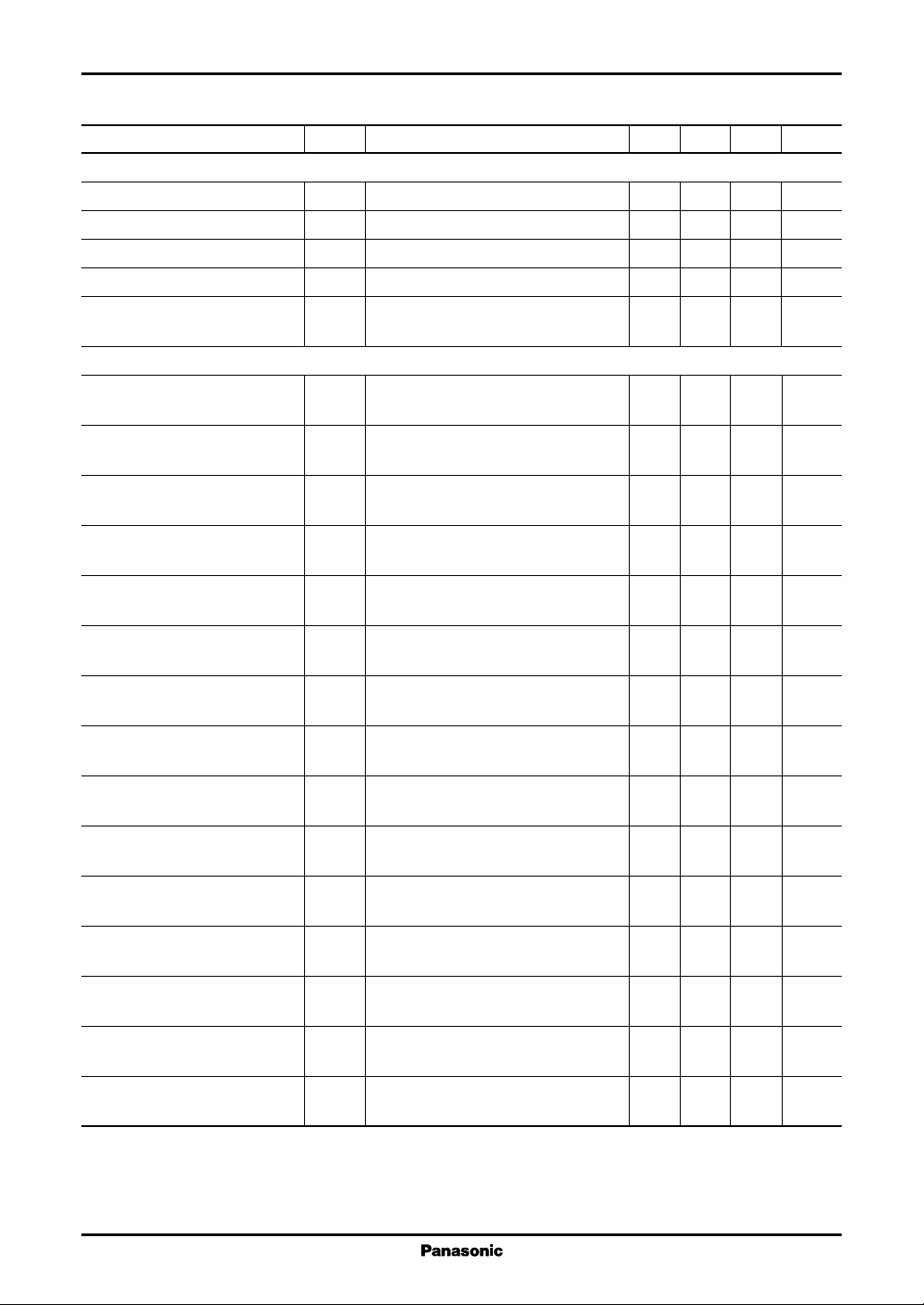
• Package: 64-SDIP, supply voltage: 5 V, 9 V
■ Applications
• Television and televideo
Unit: mm
64 33
132
(1.641)
Seating plane
58.4±0.3
1.778
0.5
+0.1
–0.05
(1.0)
SDIP064-P-0750B
17.0±0.2
3.85±0.2
(3.3)
0.7 min.
0° to 15°
5.2 max.
19.05
0.25
+0.1
–0.05
1
AN5095K ICs for T V
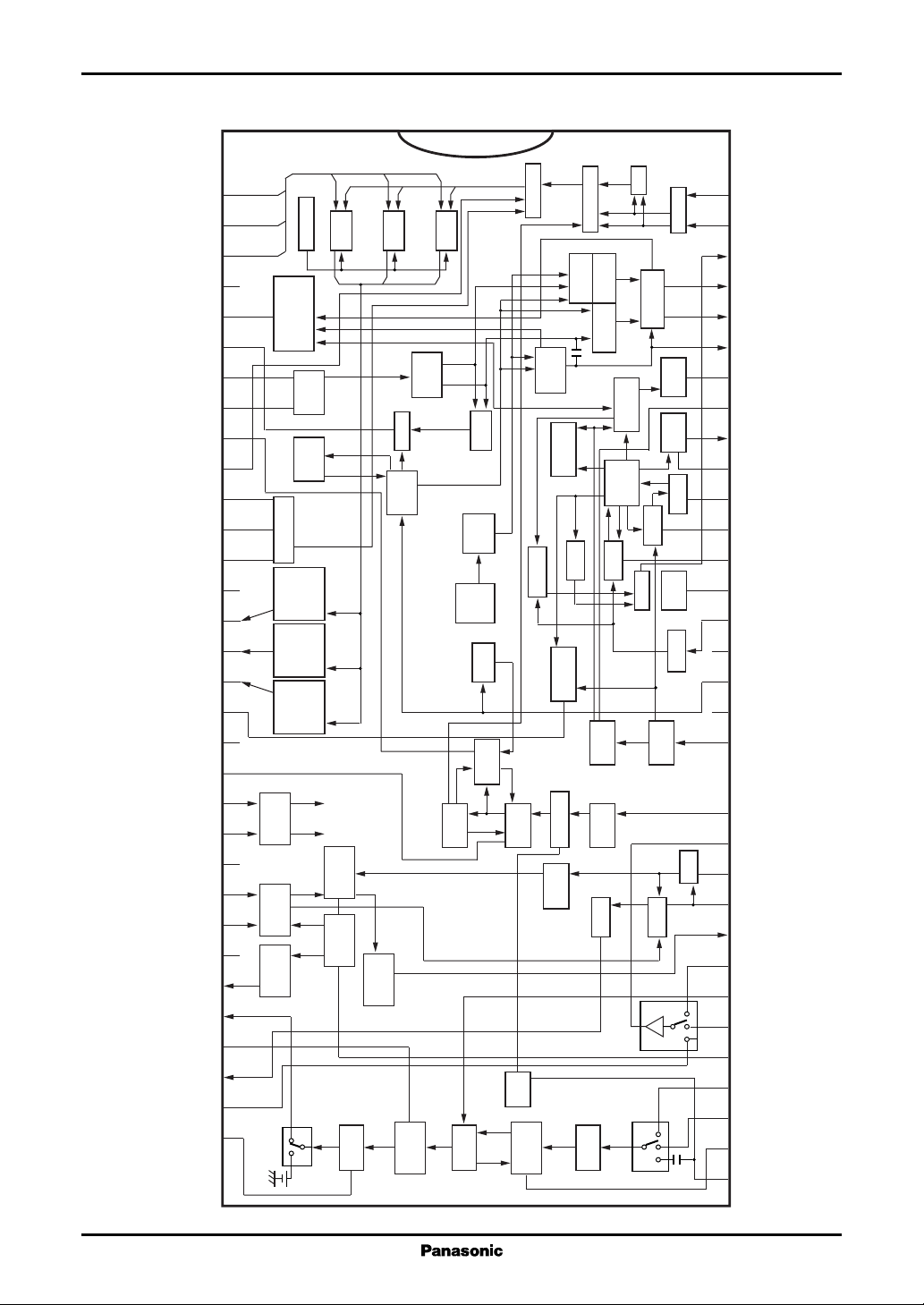
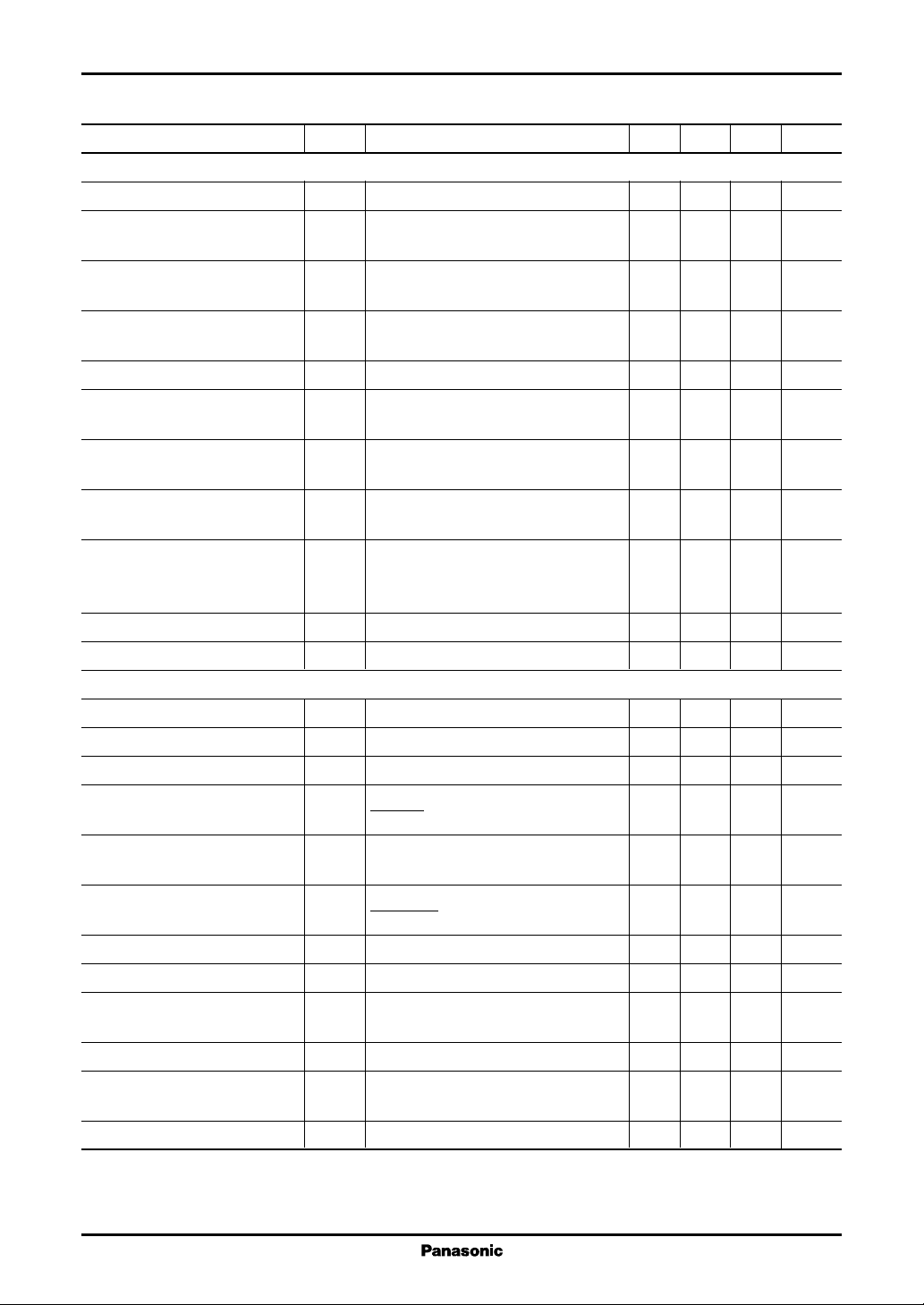
■ Block Diagram
R-clamp filter
G-clamp filter
B-clamp filter
Killer
Killer out
50 Hz/60 Hz out
SECAM det. out
APC
4.43 MHz
3.58 MHz
BL det.
Ys-in
R-in
G-in
B-in
V
(9 V)
CC1
R-out
G-out
B-out
Hor. lock det.
GND (R, G, B/DAC)
ACL
SDA
SCL
V
(VIF/SIF)
CC3
VIF1 in
VIF2 in
GND (VIF/SIF)
RF AGC
Audio out
De-emphasis
AFT
Ext. video in
De-coupling
1
2
3
4
5
6
7
8
9
10
11
12
13
14
15
16
17
18
19
20
21
22
23
24
25
26
27
28
29
30
31
32
Brightness
*
7-bit
Killer,
50 Hz/60 Hz
SECAM det. SW
Chroma
VCO
ACC
det.
(
*
6-bit)
Contrast
R
• Drive
• Cutoff
7-bit
8-bit
G
• Cutoff
8-bit
B
• Drive
• Cutoff
7-bit
8-bit
DAC
out
interface
I
2
C bus
SW
out
IF
amp.
RF
AGC
*
6-bit
*
1-bit
ASW
2-bit
R-clamp
1-bit
detect
AGC
VIF
IF
Pre-amp.
adjust
*
1-bit
Level
G-clamp
APC
ACC
amp.
*
3-bit
emphasis
generate
*
6-bit
De-
CW
B-clamp
*
1-bit
Y
clamp
VCO
Tint
FF
SW
1H
System
LPF
Black
expansion
Y
contrast
LPF
detect
R, G, B SW
Killer
ident
detect
HVBLK
lock det.
Sharpness
*
6-bit
phase
shift
SIF
Matrix
demod.
+ / −
demod.
(50 Hz/
60 Hz)
50 Hz/60 Hz
BGP
Hor.
sync. sep.
clamp
AFT
LImiter
*
*
R-Y
B-Y
2-bit
Ver.
CV
2-bit
down
AFC2
*
9-bit
*
1-bit
SIF SW
G-Y
Ver.
count down
Her.
count
*
3-bit
SCP
Video SW
*
1-bit
PN/S
SW
AFC1
sync. sep.
APC1
out
down
reg.
Hor.
Saturation Ver.
*
6-bit
Shut
H-VCO
Hor.
H-BLK
VCO
*
7-bit
64
63
62
61
60
59
58
57
56
55
54
53
52
51
50
49
48
47
46
45
44
43
42
41
40
39
38
37
36
35
34
33
-(R-Y) in
-(B-Y) in
SCP
-(R-Y) out
-(B-Y) out
SECAM interface
V
OUT
Ver. clamp
H-out
X-ray protect
H-OSC
AFC1
AFC2
V
CC2
FBP in
GND (V, C, J)
C-in
V
(V, C, J)
CC3
Sync. in
Y-in
Video out
V-OSC
APC1
Det. out
Int. Video2
SIF APC
Int. Video1
IF AGC
SIF1 in
SIF2 in
SIF regulator filter
SIF3 in/sharpness
2
ICs for TV AN5095K
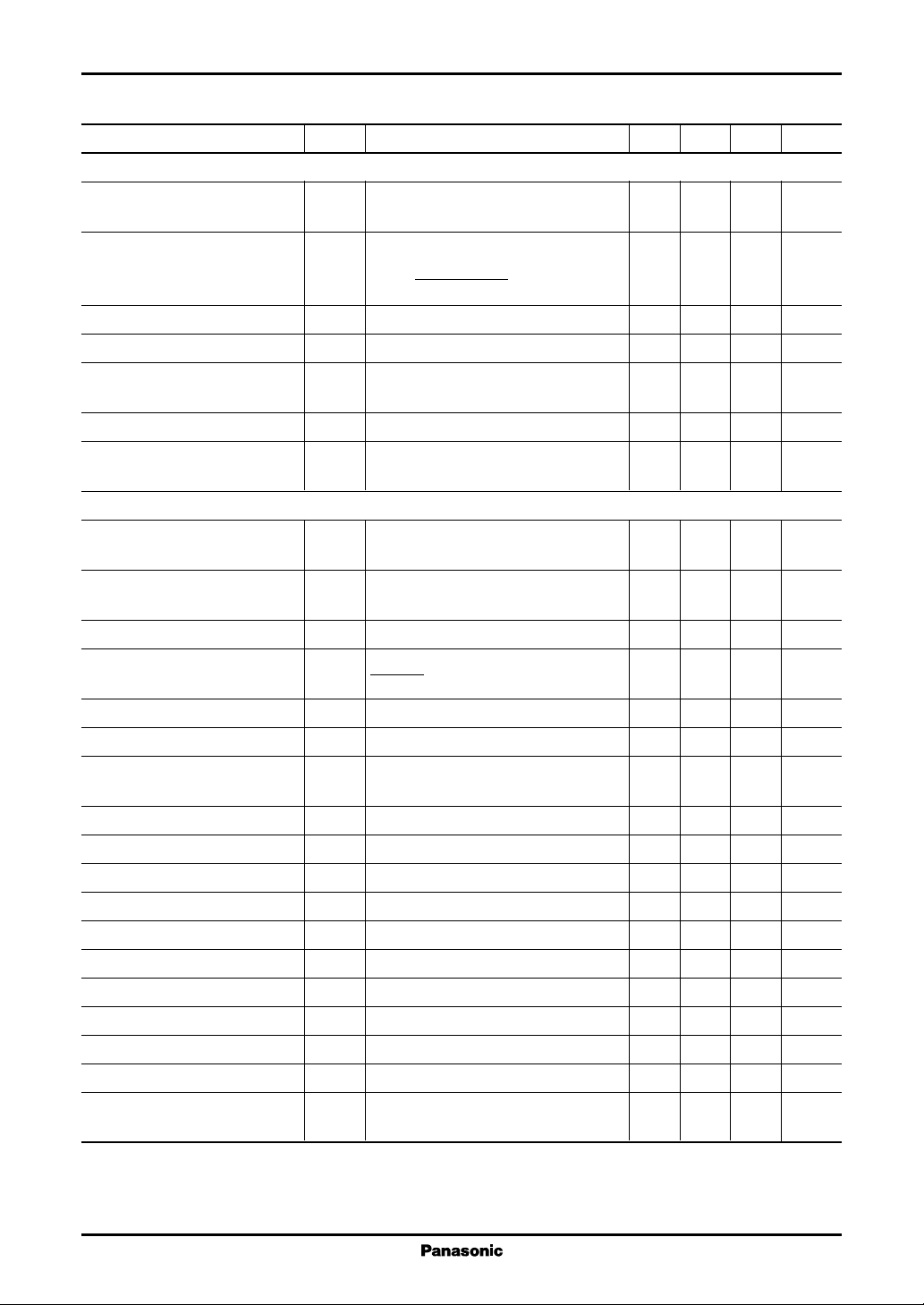
■ Pin Descriptions
Pin No. Description
Pin No. Description
1 (R) clamp
2 (G) clamp
3 (B) clamp
4 Killer filter
5 Killer out, 50 Hz/60 Hz out, SECAM det. out
6 Chroma APC filter
7 Chroma VCO (4.43 MHz)
8 Chroma VCO (3.58 MHz)
9 Black level det./Blank off SW
10 YS input (fast blanking)
11 External R-input
12 External G-input
13 External B-input
14 V
CC1
15 R-output
16 G-output
17 B-output
33 SIF3 input/sharpness
34 SIF regurator filter
35 SIF2 input
36 SIF1 input
37 IF AGC filter
38 Internal videol input
39 SIF APC filter
40 Internal video2 input
41 VIF detect output
42 VIF APC 1 filter
43 VIF VCO (fP/2)
44 Video output
45 Y-input
46 H, V sync. input
47 V
-2 (chroma/jungle/DAC)
CC3
48 Chroma input/black expansion start
49 GND (video/chroma/jungle)
18 Hor.lock detect
19 GND (R, G, B/I2C/DAC)
20 ACL
21 SDA
22 SCL
23 V
-1 (VIF/SIF)
CC3
24 VIF1 input
25 VIF2 input
26 GND (VIF/SIF)
27 RF AGC output
28 Audio output
29 De-emphasis
30 AFT output
31 External video input
32 DC De-coupling filter
50 FBP input
51 V
(hor. stability supply)
CC2
52 AFC2 filter
53 AFC1 filter
54 Hor. VCO (32 fH)
55 X-ray protection input
56 Hor. pulse output
57 Ver. sync. clamp
58 Ver. pulse output
59 SECAM interface
60 -(B-Y) output
61 -(R-Y) output
62 Sandcastle pulse output
63 -(B-Y) input
64 -(R-Y) input
3
AN5095K ICs for T V
■ Absolute Maximum Ratings
Parameter Symbol Rating Unit
Supply voltage V
Supply current I
Power dissipation
Operating ambient temperature
Storage temperature
Note)*1: Except for the operating ambient temperature, and storage temperature, all ratings are for Ta = 25°C.
2: The power dissipation shown is for the IC package in free air at Ta = 70°C.
*
*2
*1
*1
CC
CC
V
V
P
D
T
opr
T
stg
CC1 (14)
CC3 (23, 47)
I
14
I
23+47
I
51
10.5 V
6.0
67 mA
126
27
1 480 mW
−20 to +70 °C
−55 to +150 °C
■ Recommended Operating Range
Parameter Symbol Range Unit
Supply voltage V
V
Terminal voltage V
V
V
V
V
V
V
V
V
V
V
V
V
Supply current I
Circuit current I
I
I
I
I
I
CC1
CC3
5
10
11
12
13
21
22
27
30
48
50
55
59
51
15
16
17
41
44
46
8.1 to 9.9 V
4.5 to 5.5
0 to 6 V
0 to 6
0 to 6
0 to 6
0 to 6
0 to 6
0 to 6
0 to 10.5
0 to 10.5
0 to V
14
0 to V
47
0 to 2
0 to V
14
10 to 25 mA
−3.2 to +0.6 mA
−3.2 to +0.6
−3.2 to +0.6
− 0.8 to +0.8
−1.1 to +0.4
− 0.8 to +0.1
4
ICs for TV AN5095K
■ Recommended Operating Range (continued)
Parameter Symbol Range Unit
Circuit current I
Note) Do not apply external currents or voltages to any pins not specifically mentioned.
For circuit currents, '+' denotes current flowing into the IC, and '−' denotes current flowing out of the IC.
56
I
58
I
59
−6.4 to +0.1 mA
− 0.8 to +0.1
− 0.3 to +0.1
■ Electrical Characteristics at Ta = 25°C
Parameter Symbol Conditions Min Typ Max Unit
Power Supply
Supply current 1 I
Supply current 2 I
Supply current 3 I
Stabilized supply voltage V
Stabilized supply current I
Stabilized supply input resistance R
VIF circuit Typical input; fP = 38.9 MHz, V
Video detection output (typ.) V
Video detection output (max.) V
Video detection output (min.) V
Video detection output- f
frequency characteristic 1 MHz output
Synchronous peak value voltage V
APC high-level pull-in range f
APC low-level pull-in range f
RF AGC delay point adjustable ∆V
1
*
range
VCO free-running frequency ∆f
RF AGC maximum sink current I
RF AGC minimum sink current I
Note)*1 to *9: Refer to "Explanation of test methods".
Current at V
14
Current at V
23
Current at V
47
Voltage at I
51
Current at V
51
DC measurement, slant between at 1 5 10 Ω
51
I
= 10 mA and 25 mA
51
= 90 dBµ, DAC data are typical
IN
Modulation m = 87.5%, data 0B = 44 1.7 2.1 2.5 V[p-p]
PO
POmax0B
POmin0B
PC
SP
= 74 1.9 2.6 3.3 V[p-p]
= 04 1.1 1.6 2.1 V[p-p]
Frequency which becomes −3 dB for 5.5 8 12 MHz
Synchronized peak value voltage at 1.6 2.0 2.4 V
= 9 V 394857mA
14
= 5 V 7 10 13 mA
23
= 5 V 496377mA
47
= 15 mA 5.8 6.5 7.2 V
51
= 5 V 2 5 7 mA
51
V[p-0] measurement
High-pass side pull-in range 1.0 2.0 MHz
PPH
(difference from fP = 38.9 MHz)
Low-pass side pull-in range −2.0 −1.0 MHz
PPL
(difference from fP = 38.9 MHz)
Delay point in which data are 0A = 00 75 95 dBµ
RFDP
to 3F (input at V27 = approx. 6.5 V)
Dispersion without V
P
V
(IF AGC) = 0 V (measurement of
37
IN
the difference from 38.9 MHz)
Max. current IC can sink when pin 27 1.5 3.0 mA
RFmax
is low
IC leak current at which pin 27 is high − 50 0 50 µA
RFmin
−1.2 0 1.2 MHz
5
AN5095K ICs for T V
■ Electrical Characteristics at Ta = 25°C (continued)
Parameter Symbol Conditions Min Typ Max Unit
VIF circuit (continued) Typical input; fP = 38.9 MHz, V
2
AFT discrimination sensitivity
AFT center voltage V
AFT maximum output voltage V
AFT minimum output voltage V
Detection output resistance R
*
µ
∆f = ±25 kHz 40 57 75 mV/kHz
AFT
AFTV30
AFTmaxV30
AFTminV30
O41
at VIN without input 4.0 4.5 5.0 V
at f = fP −500 kHz 7.8 8.1 8.7 V
at f = fP +500 kHz 0.3 0.8 1.0 V
DC measurement, 70 120 170 Ω
IO = − 0.4 V to −1.0 mA
SIF circuit Typical input; fS = 6.0 MHz, fM = 400 Hz, V
Audio detection output V
SOP36∆f
= ±50 kHz 0.90 1.15 1.40 V[rms]
(PAL, SIF1) 0B-D3 = 0
Audio detection output V
SOP35∆f
= ±50 kHz 0.90 1.15 1.40 V[rms]
(PAL, SIF2) 0B-D3 = 0
Audio detection output V
SOP33∆f
= ±50 kHz 0.90 1.15 1.40 V[rms]
(PAL, SIF3) 0B-D3 = 0
Audio detection output R
∆f = ±25 kHz −2.5 − 0.5 1.5 dB
SN/P
NTSC/PAL 0B-D3 = 1, ratio to PAL (V
Audio detection output ∆V
= 5.5 MHz and 6.0 MHz −30 3 dB
SOPfS
linearity ratio to 6.5 MHz
SIF pull-in range f
NTSC (4.5 MHz)
SIF pull-in range f
NTSC (4.5 MHz)
SIF pull-in range f
PAL (5.5 MHz)
SIF pull-in range f
PAL (5.5 MHz)
SIF pull-in range f
PAL (6.0 MHz)
SIF pull-in range f
PAL (6.0 MHz)
SIF pull-in range f
PAL (6.5 MHz)
SIF pull-in range f
PAL (6.5 MHz)
De-emphasis terminal R
Pull-in range of high-pass side 4.8 5.0 MHz
SNH
(4.5M)
Pull-in range of low-pass side 4.0 4.2 MHz
SNL
(4.5M)
Pull-in range of high-pass side 5.8 6.0 MHz
SPH
(5.5M)
Pull-in range of low-pass side 5.0 5.2 MHz
SPL
(5.5M)
Pull-in range of high-pass side 6.3 6.5 MHz
SPH
(6.0M)
Pull-in range of low-pass side 5.5 5.7 MHz
SPL
(6.0M)
Pull-in range of high-pass side 6.8 7.0 MHz
SPH
(6.5M)
Pull-in range of low-pass side 6.0 6.2 MHz
SPL
(6.5M)
Impedance of pin 29 at PAL 32 40 48 k Ω
29P
output resistance (PAL)
De-emphasis terminal R
Impedance of pin 29 at NTSC 48 60 72 kΩ
29N
output resistance (NTSC)
Note)*1 to *9: Refer to "Explanation of test methods".
= 90 dBµ, DAC data are typical
IN
= 90 dBµ
IN
)
SOP36
6
ICs for TV AN5095K
■ Electrical Characteristics at Ta = 25°C (continued)
Parameter Symbol Conditions Min Typ Max Unit
AV SW circuit
Video SW voltage gain G
Video SW-frequency f
VSW
characteristic 1 MHz, V
Video SW external input terminal V
voltage
Video SW external output DC V
voltage 03-D7 = 1, 0B-D7 = 1
Video SW external input resistance R
Video SW output resistance R
Video SW internal clamp terminal V
voltage I
Video SW internal output DC V
voltage
Audio SW voltage gain G
Audio SW output DC voltage V
Audio SW output resistance R
Video signal processing circuit Typical input; 0.6 V[p-p] (V
Video output (typ.) V
Video output (max.) V
Video output (min.) V
Contrast variable range Y
YOmax
YOmin
Cmax/min03
Video frequency characteristic f
Picture quality variable range Y
Smax/minV33
Pedestal level (typ.) V
Pedestal variable width ∆V
Brightness control sensitivity ∆V
Video input clamp voltage V
ACL sensitivity AC L Amount of change of Y-out, when V
Blanking level V
VSWf
= 1 MHz, V
= 1 V[p-p] 5.7 6.7 7.7 dB
IN
Frequency to become −3 dB from f = 810 MHz
= 0.714 V[0-p]
IN
DC measurement 1.7 2.0 2.3 V
31
DC measurement, 4.2 4.8 5.4 V
44E
DC measurement 44 56 68 kΩ
I31
DC measurement, 110 150 190 Ω
O44
IO = − 0.6 mA to −1.0 mA
DC measurement, 1.4 1.7 2.0 V
38, 40
= −1.0 mA
IN
DC measurement 3.7 4.3 4.9 V
44I
Data 03-D7 = 1, 0B-D7 = 1, −10 1 dB
ASW
(input from outside) f = 400 Hz,
V
= 1 V[p-p]
IN
DC measurement 3.7 4.2 4.7 V
28
DC measurement 350 450 550 Ω
O28
= 0.42 V[p-p] stair-step) at G-out
BW
Data 03 = 20 (typ.) (contrast) 2.0 2.5 3.0 V[0-p]
YO
Data 03 = 3F (max.) 4.1 5.0 5.9 V[0-p]
Data 03 = 00 (min.) 0.15 0.50 1.00 V[0-p]
= 3F 15 20 25 dB
03 = 00
Pin 33 = 5 V (sharpness), frequency to 5.5 6.0 MHz
YC
become −3 dB from f = 0.2 MHz
= 7V
V
= 5V
33
Data 02 = 40 (typ.) (brightness) 2.0 2.5 3.0 V
PED
Difference between data 02 = 00 and 7F 2.15 2.75 3.35 V
PED
Average amount of change per 1-step 14 20 26 mV/Step
BRT
= 3.8 MHz
f
91317dB
between data 02 = 30 and 50
Pin 45 clamp voltage 3.2 3.7 4.2 V
YCLP
2.7 3.2 3.7 V/V
20
= 3.0 V → 3.5 V
Blanking pulse DC voltage 1.0 1.5 V
YBL
7
AN5095K ICs for T V
■ Electrical Characteristics at Ta = 25°C (continued)
Parameter Symbol Conditions Min Typ Max Unit
Video signal processing circuit (continued) Typical input; 0.6 V[p-p] (V
Service SW
*
threshold voltage
DC restoration ratio T
Video input clamp current I
Pedestal difference voltage ∆V
Brightness voltage tracking ∆T
V
YCLP
Voltage at which vertical output stops
STH
when pin 20 (ACL) voltage is decreased
APL10% to 90% 90 100 110 %
DC
∆AC − ∆DC
TDC =
∆AC
× 100
DC measurement; Sink current inside of IC
Pedestal difference voltage of R, G, B-out
IPL
Ratio of R, G, B-out fluctuation level 0.9 1.0 1.1 Time
BL
for data 02 (bright) = 20 to 60
Video voltage gain relative ratio ∆GYCOutput ratio of R, B-out against G-out 0.8 1.0 1.2 Time
Video voltage gain tracking ∆T
Ratio of gain of R, G, B-out for data 03 0.9 1.0 1.1 Time/
CONT
(contrast) = 10 to 3 0 Time
Color signal processing circuit Burst 150 mV[p-p] (PAL), reference is B-out
Color-difference output (typ.) V
Input; Color bar 2.9 3.7 4.5 V[p-p]
CO
Data 00 = 20 (typ.), 03 = 20 (typ.)
Color-difference output (max.) V
Data 03 = 3F, amplitude of one side 2 .6 3.3 V[0-p]
COmax
03 = 20
Color-difference output (min.) V
Contrast adjustable range C
Cmax/min03
Data 00 = 00, 03 = 20 100
COmin
= 3F
03 = 00
00
= 20
ACC characteristic 1 ACC1 Burst 150 mV[p-p] → 300 mV[p-p] 0.9 1.0 1.2 Time
ACC characteristic 2 ACC2 Burst 150 mV[p-p] → 30 mV[p-p] 0.8 1.0 1 .2 Time
NTSC tint center ∆θ
The difference from data 01 = 20 at −7 0 7 Step
C
which tint is adjusted to center
NTSC tint adjustable range 1 ∆θ1Input; Rainbow data 01 = 3F 30 50 65 deg
NTSC tint adjustable range 2 ∆θ2Input; Rainbow data 01 = 00 − 65 − 50 − 30 deg
Color-difference output ratio (R) R/B Input; Rainbow for both PAL/NTSC 0.46 0.56 0.66 Time
Color-difference output ratio (G) G/B Input; Rainbow for both PAL/NTSC 0.28 0.34 0.40 Time
Color-difference output angle (R) ∠R Input; Rainbow for both PAL/NTSC 78 90 102 deg
Color-difference output angle (G) ∠G Input; Rainbow for both PAL/NTSC 224 236 248 deg
PAL color killer tolerance V
NTSC color killer tolerance V
APC high-lebel pull-in range f
APC low-lebel pull-in range f
Color killer detection output V
0 dB = 150 mV[p-p] − 57 − 44 − 34 dB
KILLP
0 dB = 150 mV[p-p] − 57 − 44 − 34 dB
KILLN
Both PAL/NTSC 450 700 Hz
CPH
Both PAL/NTSC −700 − 450 Hz
CPL
V5 , killer out at which chroma input 4.5 5.0 V
KC
voltage (color) data 0A-D6 = 0, 0A-D7 =1
Note) * : Since pin 20 is also used partly as service SW when used as ACL, a sufficient care must be taken so as not to become V
< 0.9 V in carrying out set design.
= 0.42 V[p-p] stair-step) at G-out
BW
0.3 V
61116µA
− 0.2 0 0.2 V
15 20 25 dB
mV[p-p]
20
8
ICs for TV AN5095K
■ Electrical Characteristics at Ta = 25°C (continued)
Parameter Symbol Conditions Min Typ Max Unit
Color signal processing circuit (continued) Burst 150 mV[p-p] (PAL), reference is B-out
Color killer detection output V
KBWV5
voltage (B & W) data 0A-D6 = 0, 0A-D7 =1
Demodulation output -(B-Y) V
Demodulation output -(R-Y) V
Demodulation output angle ∠(B-Y)
Demodulation output angle ∠(R-Y)
CW output level (4.43 MHz)
CW output level (3.58 MHz)
CW output level period t
*
(SECAM)
3
SECAM judgment current I
SECAM judgment output V
PAL/NTSC DC level V
SECAM DC level V
DB
DR
∠RDBB-Y axis out of phase − 6 0 6 deg
∠RDRB-Y axis phase difference 84 90 96 deg
3
*
V
CWP
3
*
V
CWN
CW
SECAM
SE
59PNV59
59SV59
RGB processing circuit DAC data are typicals
Drive adjusting range G
Offset adjusting range V
Y
threshold voltage V
S
Y
threshold voltage V
S
External R, G, B pedestal ∆V
DV
CUT-OFF
YSON
YSOF
EPLYS
difference voltage
Internal and external pedestal ∆V
PL/IE
difference voltage
External R, G, B output voltage V
External R, G, B output difference
∆V
ERGB
ERGB
voltage
External R, G, B contrast variable
EC
max/min03
range
Note)*1 to *9: Refer to "Explanation of test methods".
, killer out at which chroma input 0 0.1 0.5 V
Input; Color bar measured at pin 60 555 695 835
mV[p-p]
for both PAL/NTSC
Input; Color bar measured at pin 61 430 540 650
mV[p-p]
for both PAL/NTSC
AC component, when VCO is set at 250 350 450
mV[p-p]
4.43 MHz
AC component, when VCO is set at 50
mV[p-p]
3.58 MHz
Period in which CW is outputted at 1.31 1.41 1.51 ms
SECAM, PAL
The minimum value to take out current 50 100 150 µA
from pin 59 to discriminate as SECAM
V5 , det. ou
t,
when SECAM signal input 4.5 5.0 V
data 0A-D6 = 1, 0A-D7 = 0, SECAM
DC level at PAL/NTSC 0.8 1.3 1.65 V
DC level at SECAM 4.1 4.6 5.1 V
AC change amount for R, B-out between
567dB
drive adjustment max. and min.
DC change amount for R, G, B-out 2.2 2.5 2.8 V
between offset adjustment max. and min.
Minimum DC voltage at which Y
S
1.0 V
turns on
Maximum DC voltage at which Y
S
0.4 V
turns off
= 1 V is applied − 200 0 200 mV
Internal part external part − 200 0 200 mV
Input 0.7 V[p-p], contrast 03 = 20 (typ.) 1.8 2.2 2.7 V[p-p]
Input 0.7 V[p-p], contrast 03 = 20 (typ.) 0.8 1.0 1.2 Time
= 3F 12 17 22 dB
03 = 00
9
AN5095K ICs for T V
■ Electrical Characteristics at Ta = 25°C (continued)
Parameter Symbol Conditions Min Typ Max Unit
RGB processing circuit (continued) DAC data are typicals
External R, G, B frequency f
characteristic
Internal and external R, G, B V
output voltage ratio 0.6 V[p-p] input, contrast 03 = 20 (typ.)
Synchronizing signal processing circuit
Horizontal free run frequency f
Horizontal output pulse duty cycle τ
Horizontal pull-in range f
PAL horizontal free run frequency f
NTSC vertical free run frequency f
Vertical output pulse width τ
PAL vertical pull-in range f
NTSC vertical pull-in range f
Horizontal high-level output voltage
Horizontal low-level output voltage
Vertical high-level output voltage V
Vertical low-level output voltage V
Screen center variable range ∆T
Overvoltage protection operation V
voltage H-out does not appear any longer
Vertical frequency f
discrimination (50) low (< 0.5 V)
Vertical frequency f
discrimination (60) high (> 4.5 V)
Synchronous signal clamp voltage V
Horizontal output start voltage V
I2C interface
Sink current when ACK I
SCL, SDA signal high level input V
SCL, SDA signal low level input V
Allowable maximum input f
frequency
Input 0.2 V[p-p] 8 10 MHz
RGBC
External part 0.7 V[p-p]/internal part 0.78 0.92 1.06 Time
E/I
Without sync. signal input 15.33 15.63 15.93 kHz
HO
Upward pulse duty cycle 31 37 43 %
HO
Difference from fH = 15.625 kHz ± 500 ± 650 Hz
HP
Data 01-D7 = 1, 02-D7 = 0, forced 48 50 52 Hz
VO-P
50 Hz mode, without sync. signal input
Data 01-D7 = 1, 02-D7 = 1, forced 5 8 60 62 Hz
VO-N
60 Hz mode, without sync. signal input
For both PAL/NTSC 9 10 11 1/fH
VO
VPPfH
VPNfH
V
56H
V
56L
58H
58L
= 15.625 kHz, forced 50 Hz mode 46 54 Hz
= 15.75 kHz, forced 60 Hz mode 56 64 Hz
High-level DC voltage 2.8 3.1 3.4 V
Low-level DC voltage 0.3 V
High-level DC voltage 3.9 4.2 4.5 V
Low-level DC voltage 0.3 V
Change amount of phase difference between
HC
2.6 3.2 4.4 µs
sync. and H-out of data 0B = 40 to 47
The pin 55 minimum voltage at which 0.60 0.68 0.76 V
X-RAY
Vertical frequency at which V5 becomes
50
Vertical frequency at which V5 becomes
60
V46 clamp voltage 1.1 1.4 1.7 V
46
The minimum V50 at f0 > 10 kHz 3.4 4.2 5.0 V
fHS
47 55 Hz
57 63 Hz
and horizontal oscillation output is
higher than 1 V[p-p]
The maximum value of pin 21 sink 1.5 2.0 5.0 mA
ACK
current at ACK
IHI
ILO
Imax
3.1 V
0.9 V
100 kbit/s
10
ICs for TV AN5095K
■ Electrical Characteristics at Ta = 25°C (continued)
• Design reference data
Note) The characteristics listed below are theoretical values based on the IC design and are not guaranteed.
Parameter Symbol Conditions Min Typ Max Unit
VIF circuit Typical input; fP = 38.9 MHz, VIN = 90 dBµ
Input sensitivity V
Maximum allowable input V
SN ratio SN
Differential gain DG
Differential phase DP
4
Black-noise detection level
Black-noise clamp level
*
∆VBNDifference from sync. peak value − 45 IRE
4
*
∆V
RF-AGC operation sensitivity G
VCO switch-on drift ∆f
5
Inter modulation
*
RF-AGC adjustment sensitivity S
AFT offset adjustment sensitivity S
Video detection output fluctuation ∆V
with V
CC
Video detection output- ∆V
temperature characteristics
Input resistance (pin 24, pin 25) R
Input capacitance (pin 24, pin 25) C
Sound-IF output level V
VCO control sensitivity β
VCO adjustment range f
RF-AGC delay point-temperature ∆V
characteristics
VCO free-running frequency- ∆f
temperature characteristics
AFT center frequency-temperature ∆f
characteristics voltage becomes 4.5 V, Ta = −20°C to
External mode output DC voltage V
Note)*1 to *9: Refer to "Explanation of test methods".
Input level at which V
PS
Input level at which V
Pmax
P
P
P
Difference from sync. peak value 45 IRE
BNC
Input level difference, when V
RF
becomes −3 dB
PO1
becomes +1 dB
PO1
45 dBµ
110 dBµ
50 dB
5%
5 deg
= 1 V 0.5 3.0 dB
27
goes to 7 V
Frequency drift from 5 sec. to 5 min. after 200 kHz
PD
SW-on
IM V
RF
AFT
P/VVCC
P/TTa
I24,25
I24,25
SIFfS
P
VCO
− V
fC
= −2 dB, V
fP
− V
= −12 dB 46 dB
fS
fP
Output voltage in data 1-step, 1 4 V/step
average change amount of V
27
Output voltage in data 1-step, 0.1 0.3 V/step
average change amount of V
30
= ±10% ±15 %
= −20°C to +70°C ±10 %
f = 38.9 MHz 1.2 kΩ
f = 38.9 MHz 4.0 pF
= 38.9 MHz − 6.0 MHz, P/S = 20 dB 90 110 dBµ
∆V42 = ±0.1 V 2.0 3.5 kHz/mV
Free-running frequency change width 3 5 MHz
at data 0C = 00 to 7F
DP/TTa
P/TTa
AFT/T
= −20°C to +70°C 5dB
= −20°C to +70°C 300 kHz
Input frequency at which AFT output 300 kHz
+70°C
Output DC voltage at AV-SW 0.5 1.0 1.8 V
41EXT
outside mode
11
 Loading...