


Panasonic AN4250S, AN4250 Datasheet
AN4250, AN4250S, AN6593
Single Low Power Consumption Operational Amplifiers
■ Overview
The AN4250, the AN4250S, and the AN6593 are
single operational amplifiers which can be operated
with very lo w power consumption. Moreover , they ha ve
wide range (±1V to±18V)of supply voltage, and
electrical characteristics such as power consumption
and input bias current can be programmed according
to the current value set by outer resistor.
They are suitable for applications to various
electronic circuits such as portable electronic
equipments operated by the battery.
■ Features
• Wide supply voltage rang (±1V to ±18V)
• Electrical characteristics programmable by set current
• Phase compensation circuit built in
• Output short-circuit protection
• Offset null
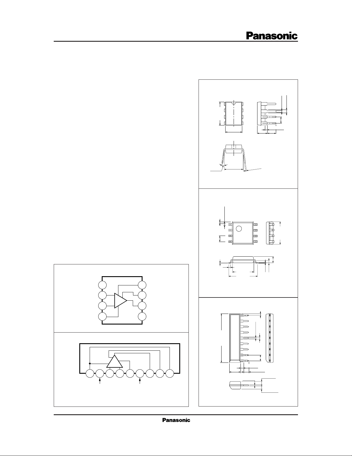
AN4250
1
2
3
9.4±0.3
4
3—15˚
8-pin DIL Plastic Package (DIP008-P-0300B)
±0.3
6.3
7.62±0.25
8
7
6
5
0.15
AN4250S
0.4±0.25
1
0.6±0.31.27
2
3
4
3.8±0.25
+0.1
– 0.05
8
7
6
5
0.51min.
(3.45)
Unit:mm
0.5±0.1
1.2±0.25
2.54
Unit:mm
5.0±0.3
■ Block Diagram
AN4250, AN4250S
Offset
Null
V
in
V
in
V
EE
AN6593
1 25436789
I
SET
Note) Pin1 and Pin9 are common.
–
+
Offset
Null
1
2
3
4
–
–
V
in
–
+
+
+
V
V
EE
in
Offset
Null
0.1±0.1
0.3
4.2±0.3
6.5±0.3
I
8
SET
7
V
CC
6
V
O
Offset
5
Null
I
V
V
O
SET
CC
8-pin PANAFLAT Plastic Package (SOP008-P-0225A)
9
8
7
6
0.5±0.1
5
1.0±0.25
0.3
+ 0.1
– 0.05
4
3
2
1
2.7±0.25
21.7±0.3
4.3±0.3
9-pin SIL Plastic Package (SIP009-P-0000A)
0.15
0.65
0.4±0.25
1.2±0.25
2.54
1.4±0.25
1.35±0.25
1.5±0.2
Unit:mmAN6593
■ Pin Descriptions
〈AN4250, AN4250S〉
Pin No.
1
Offset null
2
Inverting input
3
Non inverting input
(GND)
4
V
EE
Offset null
5
Output
6
V
7
CC
I
8
SET
Pin name
〈AN6593〉
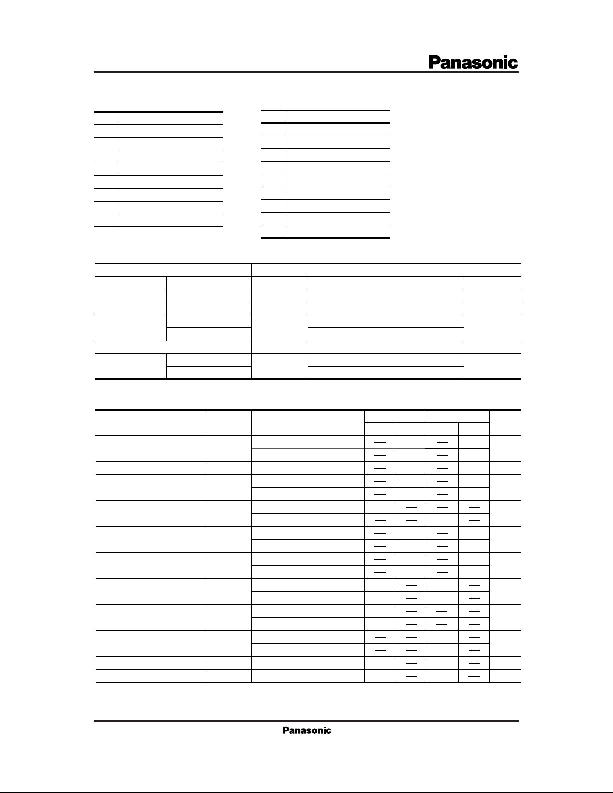
■ Absolute Maximum Ratings (Ta=25˚C)
Parameter Symbol Rating Unit
Supply voltage
Voltage
Power dissipation
Operating ambient temperature
Storage
temperature
Differential input voltage
Common-mode input voltage
AN4250, AN6593
AN4250S
AN4250, AN6593
AN4250S
Pin No.
1
I
SET
Offset null
2
Inverting input
3
Non inverting input
4
V
5
EE
Offset null
6
Output
7
V
8
CC
I
9
SET
V
CC
V
ID
V
ICM
P
D
T
opr
T
stg
(GND)
Pin name
±18
±30
±15
500
360
–20 to +75
–50 to +150
–50 to +125
V
V
V
mW
˚C
˚C
■ Electrical Characteristics (VCC=15V, VEE=–15V, Ta=25˚C)
Parameter Symbol Condition
<
100kΩ
R
S
Input offset voltage
Input offset current
Input bias current
Large signal voltage gain
Supply current
Power consumption
Input voltage range
Maximum output voltage
Maximum output voltage
Common-mode rejection ratio
Supply voltage rejection ratio
V
I (offset)
I
IO
I
Bias
G
V
I
CC
P
C
V
CM
V
O (max.)
V
O (max.)
CMR dB
SVR dB
=
±
=±1.5V, R
V
±
=±1.5V
V
S
<
=
100kΩ
VO=±10V, RL=100kΩ
=±10V, RL=10kΩ
V
O
V±=±1.5V
±
=±1.5V
V
±
=±1.5V
V
RL=100kΩ
V±=±1.5V, RL=100kΩ
RL=10kΩ
V±=±1.5V, RL=10kΩ
<
10kΩ
R
S
=
10kΩ
R
<
S
=
=1µAI
I
SET
min
max min max
5
5
6
10
10
96
11
8
330
24
±13.5
±0.6
±12
±0.6
70
74
SET
96
±13.5
±0.6
±12
±0.6
70
74
=10µA
100
3000
270
Unit
6
mV
6
nA
20
75
nA
75
dB
µA
90
µW
V
V
V