

Panasonic AN3986FHP, AN3986FBP Datasheet
1
ICs for Video Camera
■ Overview
The AN3986FBP and the AN3986FHP are stereo audio
signal processor ICs for 8-mm camcorder. It incorporates
all the functions needed for stereo-audio signal processing in 8mm camcorder.
■ Features
•
Built-in headphone amplifiers
•
Built-in matrix signal processing
AN3986FBP, AN3986FHP
Stereo Audio Signal Processor ICs for 8-mm Camcorder
Supply voltage
Power dissipation
Note 2)
Operating ambient temperature
Note 1)
Storage temperature
Note 1)
V
CC
P
D
T
opr
T
stg
V
CC1
=6 / V
CC2
=9.5
392
–20 to + 70
–55 to + 125
V
mW
˚C
˚C
Parameter Symbol Rating Unit
Note 1) Ta=25˚C except operating ambient temperature and storage temperature unless otherwise specified.
Note 2) Allowable power dissipation of the package at Ta=70˚C.
AN3986FHP
Supply voltage
Power dissipation
Note 2)
Operating ambient temperature
Note 1)
Storage temperature
Note 1)
V
CC
P
D
T
opr
T
stg
V
CC1
= 6 / V
CC2
= 9.5
474
– 20 to + 70
– 55 to + 125
V
mW
˚C
˚C
Parameter Symbol Rating Unit
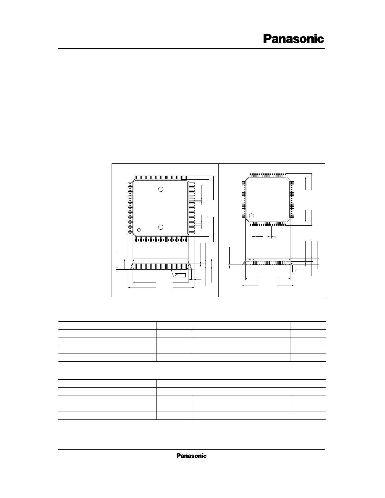
■ Absolute Maximum Ratings
AN3986FBP
Unit : mm
21.2±0.2
18.0±0.2
3.3max.
1.55±0.11.55±0.1
0.15
+ 0.1
– 0.05
211
22
18.0±0.2
21.2±0.2
0.1
(0.6)
3.4
+ 0.15
– 0.3
0.1±0.1
0.8 0.35
+ 0.1
– 0.05
42
4363
64
84
AN3986FBP
84-Pin QFH Package (QFH084-P-1818)
AN3986FHP
Unit : mm
12.0±0.2
14.0±0.2
1
0.5
0.2
+ 0.1
– 0.05
0.15
1.3±0.1
2.8±0.2
0.1±0.1
12.0±0.2
14.00.2
80-Pin QFH Package (QFH080-P-1212)
(0.5)
(min0.25)
1.3±0.1
2
ICs for Video Camera
AN3986FBP, AN3986FHP
+
10µF
10µF
+
2.2µF
0.01µF
50kΩ
VR
10kΩ
5.6kΩ
4.7µF
47µF4.7µF
4700pF
4700pF
+
4.7µF
+
4.7µF
100
µF
+
4.7µF
0.01µF
+
1µF
+
4.7µF
10µF
65 41
22
40
39
38
37
36
35
34
33
32
31
30
29
28
27
26
25
24
23
4445464748495051525354555657585960616263
2019181716151413121110987654321
V
CC
Rch
Output
Convert
+
6.8kΩ
0.01µF
0.01µF
BPF
1µF
0.01µF
0.01µF
0.01µF
0.047µ
F
ST
MONO
BIL
ST
to Control
to Control
to FMOUT
330pF
0.01
µF
33kΩ
MM
+
MUTE
8.2k
Ω
0.01µF
BPF
0.01µF
LIM
LPF
HOLD
PC
VCO
AL
+
10µF
+
–
10µF
+
2.2µF
0.01µF
–+
–+
–+
LP empha
R
+
–
R
LS CCA
50kΩ
VR
10kΩ
5.6kΩ
4700pF
4.7
µF
+
47µF4.7µF
LFP
4700pF
4700pF
R
R
R
R
R
RR
Matrix
to Control
+
4.7µF
AGC
Fade
LPF
LPF
Vo1
+
47µF
V
REF
+
100µF
++
4.7µF+47µF
V
REFH
+
100µF
0.01µF
4.7µF
+
+
100µF
0.01µF
+
+
4.7µF
10kΩ
VR
R
V
CCH
4700pF
+
+
Control
VCO Adjust (R)
FMOUT (R)
ST/MONO Time constant
HOLD 1
HOLD 2
Timing making
PG GND
PG Input
MUTE Time constant
MUTE detection
FMOUT (L)
VCO Adjuse (R)
0.01µF
Input 3 (R)
HP Vol Control
Input 2 (R)
Input 1 (R)
V
CC
(4.75V)
HP Output (R)
HP GND (R)
Line Output (R)
V
CCH
(8.2V)
V
REFH
Line Output (L)
HP GND (L)
HP Output (L)
V
REF
Input 1 (L)
AGC Time Constant
Input 2 (L) Input 3 (L)
PB/Rec Change (PB )
H
Fade Control
R
43
21
64 42
R
+
M
U
T
E
1/2/3
H
GND
Bil
MONO
ST
I
O
Detect Output
Input
change
S
P
L
/R/
ST
ON
Auto
OFF
H
GND
I
O
Output
change
Matrix
Control
to Pin37
1 2
3
4 5 6 7 8 9 10 11 12 13 14
15
17 18 19
2016
21
22
23
24
25
26
27
28
29
30
31
32
33
34
35
36
37
38
39
40
4142434445
464748495051525354555657
58
5960
616662
63
64
65
66
67
68
69
70
71
72
73
74
75
76
77
78
79
80
84
77
78
79
80
81
82
83
67
68
69
70
71
72
73
74
75
76
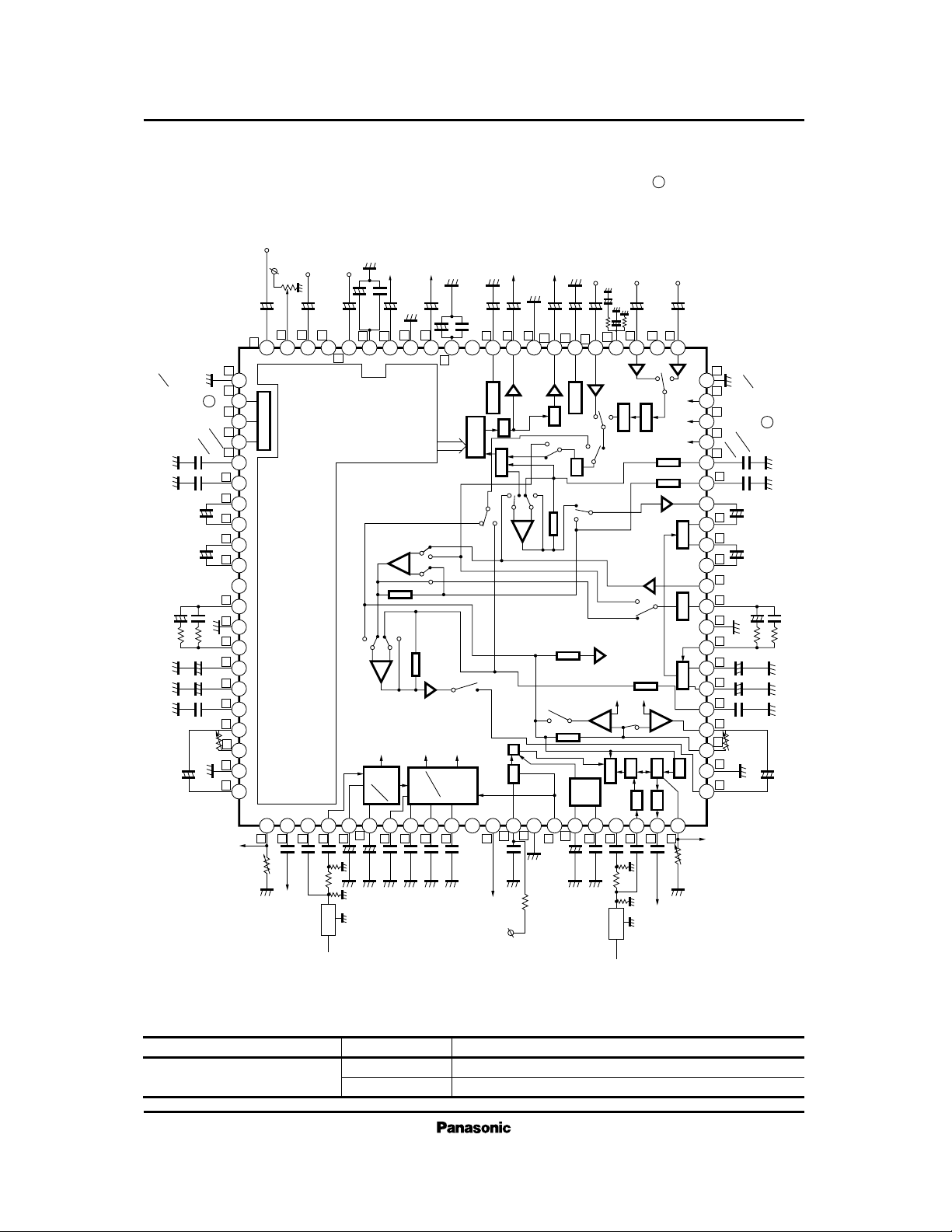
Note) A number with a circle denotes a pin
No. of the AN3986FBP, while a
number with a square denotes a pin
No. of the AN3986FHP.
■ Block Diagram
Parameter Symbol Range
Operating supply voltage range
V
CC1
V
CC2
4.5V to 5.5V
4.5V to 9.0V
■ Recommended Operating Range (Ta=25˚C)
3
ICs for Video Camera
AN3986FBP, AN3986FHP
Pin No.
Pin name
Pin No.
Pin name
43
44
45
46
47
48
49
50
51
52
54
55
56
57
58
59
60
61
62
63
64
65
66
67
68
69
70
71
72
73
75
76
77
78
79
80
81
82
83
84
NR input/output
GND
Dev. adjustment 1
Dev. adjustment 2
LP emphasis
Level sensor timing C1
Level sensor timing C2
Level sensor input
GND
LPF output
CCA amp. input
CCA output
CCA input
Buffer output
FM emphasis
NR emphasis
Mode discriminator output
Mute control
Input change switch
GND
Input 3
Rec/PB switching
Input 2
AGC time-constant
Input 1
V
REF
Headphone output
Headphone GND
Line output
V
REF
H
V
CC2
Line output
Headphone GND
Headphone output
V
CC1
Input 1
Fade control
Input 2
Headphone volume control
Input 3
GND
SP/EP mode switching
Output switching control
Matrix control
NR emphasis
FM emphasis
Buffer input
CCA input
CCA output
CCA amp. input
LPF output
GND
Level sensor input
Level sensor timing C2
Level sensor timing C1
LP emphasis
Dev. adjustment 2
Dev. adjustment 1
GND
NR input/output
VCO frequency adjustment
FM modulator output
FM demodulator input
FM detector input
FM input AGC detection
ST/MON time-constant
HOLD 2
HOLD 1
ST/MON detection
Bilingual timing generation
V
CC1
(FM)
Mono/multi time-constant
GND (PG)
PG input
MUTE time-constant
MUTE detection
FM detection input
FM demodulator input
FM modulator output
VCO frequency adjustment
■ Pin Descriptions
(L)
(L)
(L)
(L)
(L)
(L)
(L)
(L)
(L)
(L)
(L)
(L)
(L)
(L)
(L)
(L)
(L)
(L)
(L)
(L)
(L)
(R)
(R)
(R)
(R)
(R)
(R)
(R)
(R)
(R)
(R)
(R)
(R)
(R)
(R)
(R)
(R)
(R)
(R)
(R)
(R)
(R)
(R)
(R)
(R)
(L)
(L)
(L)
(L)
1
2
3
4
5
6
7
8
9
10
11
12
13
14
15
16
17
18
19
20
21
22
23
24
25
26
27
28
29
30
31
32
33
34
35
36
37
38
39
40
41
42
43
44
45
46
47
48
49
50
51
52
53
54
55
56
57
58
59
60
61
62
63
64
65
66
67
68
69
70
71
72
73
74
75
76
77
78
79
80
AN3986FHP AN3986FBP AN3986FHP AN3986FBP
1
2
3
4
5
6
7
8
9
10
12
13
14
15
16
17
18
19
20
21
22
23
24
25
26
27
28
29
30
31
33
34
35
36
37
38
39
40
41
42
Note) Pins11, 32, 53, and 74 of the AN3986FBP are to be left open.
4
ICs for Video Camera
AN3986FBP, AN3986FHP
Parameter Symbol Condition min typ max Unit
I
R35
Circuit current 1 at recording 58 73 88 mA
I
R31
Circuit current 2 at recording 1.6 2.4 mA
I
P35
Circuit current 1 at playing back
61
93 mA
2.0
77
I
R31
Circuit current 1 at playing back
1.6
2.4 mA
2.0
Line AGC output level Lch, Rch
V
OALL
V
OALR
– 8 – 7 – 6 dBs
Line AGC output distortion factor Lch, Rch
T
HALL1
T
HALR1
0.02 0.1 %
AGC ON output level Lch, Rch
V
OALL2
V
OALR2
– 4 – 1 + 2 dBs
AGC ON output distortion factor Lch, Rch
T
HALL2
T
HALR2
0.2 0.4 %
Line AGC output noise Lch, Rch
V
NALL
V
NALR
– 78 – 74 dBs
Fade control maximum attenuation
output Lch, Rch
V
FALL
V
FALR
– 80 – 75 dBs
Line through monitor output level
Lch, Rch
V
O1LL
V
O1LR
– 8 – 7 – 6 dBs
Line through monitor output noise
Lch, Rch
V
NLLL
V
NLLR
– 81 – 77 dBs
Between inputs between channels
crosstalk
– 78 – 74 dB
V
CTIN
E-E monitor output frequency
characteristics Lch, Rch
V
OLFL
V
OLFR
– 5.5 – 2.5 dBs
HP output level VOL= CENTER
Lch, Rch
V
HC8L
V
HC8R
– 28 – 26 – 24 dBs
HP output distortion factor
VOL= CENTER Lch, Rch
T
HHC8L
T
HHC8R
0.05 0.5 %
HP output level VOL= MAX Lch, Rch
V
HH8L
V
HH8R
– 18 – 16 – 14 dBs
HP output level VOL= MIN Lch, Rch
V
HL8L
V
HL8R
– 96 – 92 dBs
HP output noise voltage VOL= MIN
Lch, Rch
V
NHCOL
V
NHCOR
– 96 – 92 dBs
HP maximum output level
VOL= CENTER Lch, Rch
V
MHH8L
V
MHH8R
– 18 dBs
– 18 – 15 – 12 dBs
0.4 %
– 21 – 19 dB
0.2
– 20
3.8 5.8 dB
4.8
LP encode f characteristics Lch, Rch
V
FLRLL
V
FLRLR
2.0 3.0 4.0 dB
Encode output noise Lch, Rch
V
NRRL
V
NRRR
– 55 – 51 dB
ST/BIL level difference L + R Lch
– 0.5 0 + 0.5 dB
ST/BIL level difference L – R Lch
– 30 – 17.5 dB
Encode output level Lch, Rch
Encode output distortion factor Lch, Rch
Encode linearity Lch, Rch
SP encode f characteristics Lch, Rch
V
BSRLR
V
BSRLL
V
FORLL
V
FORLR
V
OXLL
V
OXLR
T
HORLL
T
HORLR
V
ORLL
V
ORLR
MON/BIL level difference Lch – 0.5 0 + 0.5 dB
Decode reference output level Lch, Rch
V
OLPL
V
OLPR
– 9.5 – 7 – 4.5 dB
V
CC1
= 4.75V, when no signal input
V
CC2
= 8.20V, when no signal input
V
CC1
= 4.75V, when no signal input
V
CC2
= 8.20V, when no signal input
VIN=
20dBs
f= 400Hz
V
IN
=
20dBs
f= 1kHz, THD 5th
V
IN
=
– 2dBs
f= 400Hz
V
IN
=
– 2dBs
f= 1kHz, THD 5th
No input A curve filter
No input A curve filter
V
IN
= –
20dBs, 1kHz
A curve filter
No input A curve filter
V
IN
= –
20dBs, 400Hz
VIN= –
14dBs, 1kHz
A curve filter
V
IN
= –
20dBs
ratio of 40kHz/40Hz
V
IN
= –
20dBs, 400Hz
8Ω load
V
IN
= –
20dBs, 1kHz
8Ω load, THD 5th
V
IN
= –
20dBs, 400Hz
8Ω load
V
IN
= –
20dBs, 400Hz
8Ω load
1kHz, at 1% distortion,
8Ω load THD 5th
V
IN
= –
20dBs, 400Hz
BIL mode
VIN= –
20dBs, 1kHz
to THD 5th
VIN= –
11.2/–51.2BS
f= 400Hz
VIN= –
20dBs
f= 10kHz/400Hz
V
IN
= –
20dBs, 10kHz
ratio of LP/SP
No input A curve filter
V
IN
= –
20dBs, 400Hz
V
IN
= –
20dBs, 400Hz
30kHz LPF
V
IN
= –
20dBs, 400Hz
V
OLL
, input V
ORLR
V
BMRLL
■ Electrical Characteristics (cont.) (V
CC1
= 4.75V, V
CC2
= 8.2V, Ta= 25±2˚C) (AN3986FHP)
5
ICs for Video Camera
AN3986FBP, AN3986FHP
■ Electrical Characteristics (cont.) (V
CC1
= 4.75V, V
CC2
= 8.2V, Ta= 25±2˚C) (AN3986FHP)
Decode reference output distortion
factor Lch, Rch
T
HOLPL
T
HOLPR
0.12 0.3 %
Decode linearity Lch, Rch
V
OXPL
V
OXPR
– 63 – 60 – 57 dB
Decode output noise Lch, Rch
– 87 – 79 dBs
Crosstalk Lch, Rch, at playback
C
ERL
C
ERR
– 79 dBs
Maximum output level Lch, Rch,
at playback
V
OLML
V
OLMR
0.4 1.0 %
Line mute attenuation quantity Lch, Rch
V
MLML
V
MLMR
– 92 – 87 dBs
Encode channel crosstalk Lch, Rch
S
ERL
S
ERR
– 50 – 47 dBs
E–E system monitor output channel
balance
– 0.55 0 + 0.55 dB
Encode output channel balance
Decode output channel balance
VCO free-run frequency Lch
VCO free-run frequency Rch
VCO output amplitude voltage Lch
VCO output amplitude voltage Rch
VCO 2nd harmonics output Lch
VCO 2nd harmonics output Rch
VCO reference frequency deviation Lch
VCO reference frequency deviation Rch
0
0
1.50
1.70
500
450
– 50
– 50
– 50
– 50
+ 2
+ 3
1.65
1.85
548
493
–35
–35
– 40
– 40
dB
dB
MHz
kHz
mV
P–P
mV
P–P
dB
dB
dB
dB
B
RE
B
LP
F
OL
F
OR
V
79
V
62
V
79–2
V
62–2
V
79–3
V
62–3
B
AL
V
NLPL
V
NLPR
90 120 150 kHz
45 60 75 kHz
96 110 128 kHz
–128 –110 – 96 kHz
48 55 64 kHz
– 48 kHz
Boost start time Lch, Rch,
at recording
200 µs
Boost level Lch, Rch
69dB
F
DOL
F
DRMX2
F
DLMX1
F
DOR
F
DRMX1
F
DLMX2
V
BSL
V
BSR
T
BSL
T
BSR
– 64 – 55
– 2
–3
1.35
1.55
456
410
Boost width Lch, Rch
1.1 1.3 1.5 ms
Reference FM modulation distortion
factor Lch, Rch
0.3 %
FM demodulation output Lch
–18 –15 –12 dBs
FM demodulation output Rch
–18 –15 –12 dBs
V
DER1
V
DEL1
T
BEL
T
BER
T
HDL
T
HDR
0.3 %
FM demodulation output distortion ratio
Lch
T
HDEL1
V
ORLL
, input V
ORLR
Vin= –11.6/ – 41.6dBs
f= 400Hz
No input A curve filter
V
IN
= – 20dBs, 1kHz
A curve filter
V
IN
= –10dBs, 1kHz
THD 5th
V
IN
= – 20dBs, 1kHz
A curve filter
V
IN
= –14dBs, 1kHz
A curve filter
V
OALR/VOALL
∆V= ±195.2mV
(–15dBs equivalent)
∆V= ±195.2mV
(–15dBs equivalent)
input ∆V= – 617mV
(–5dBs equivalent)
input ∆V= + 617mV
(–5dBs equivalent)
input ∆V= – 617mV
(–5dBs equivalent)
input ∆V= + 617mV
(–5dBs equivalent)
time from PG input
level difference due to gain-up
time of gain-up
Vin= –15dBs, f=1kHz
THD 5th after demodulation
DEV= ± 30kHz
fm= 400Hz
DEV= ± 60kHz
fm= 400Hz
DEV= ± 60kHz
fm=1kHz
DEV= ± 30kHz
fm=1kHz
Vin= 30mV
P–P
as 0dB
f=1.5MHz
0.3 %
–11 –14 –18 dB
FM demodulation output distortion ratio
Rch
Dropout detection ON level
T
HDER1
DODON
Parameter Symbol Condition min typ max Unit
VCO reference frequency deviation Lch
VCO reference frequency deviation Rch
Maximum frequency deviation 1 Lch
Maximum frequency deviation 2 Lch
Maximum frequency deviation 1 Rch
Maximum frequency deviation 2 Rch
V
ORLR/VORLL
V
OLPR/VOLPL
R= 8.2kΩ
R= 6.8kΩ
when f= 1.5MHz
when f= 1.7MHz
fundamental wave as 0dB
fundamental wave as 0dB
fundamental wave as 0dB
fundamental wave as 0dB
 Loading...