

Panasonic AN3861SA Datasheet
■ Overview
The AN3861SA is a sensor-less motor drive IC for VTR
movie cylinder. It uses both sensor-less and sine wave drive,
thus excellent for low-noise applications.
■ Features
•
Operating supply voltage range : VCC=3.0 to 5.5V, VB=4.0 to
10.5V
•
Reduced magnetosound using 3-phase full-wave overlap
drive. Built-in power transistor.
•
Standby mode for minimizing power consumption
•
Voltage output for controlling SW power supply
•
Motor neutral point input terminal
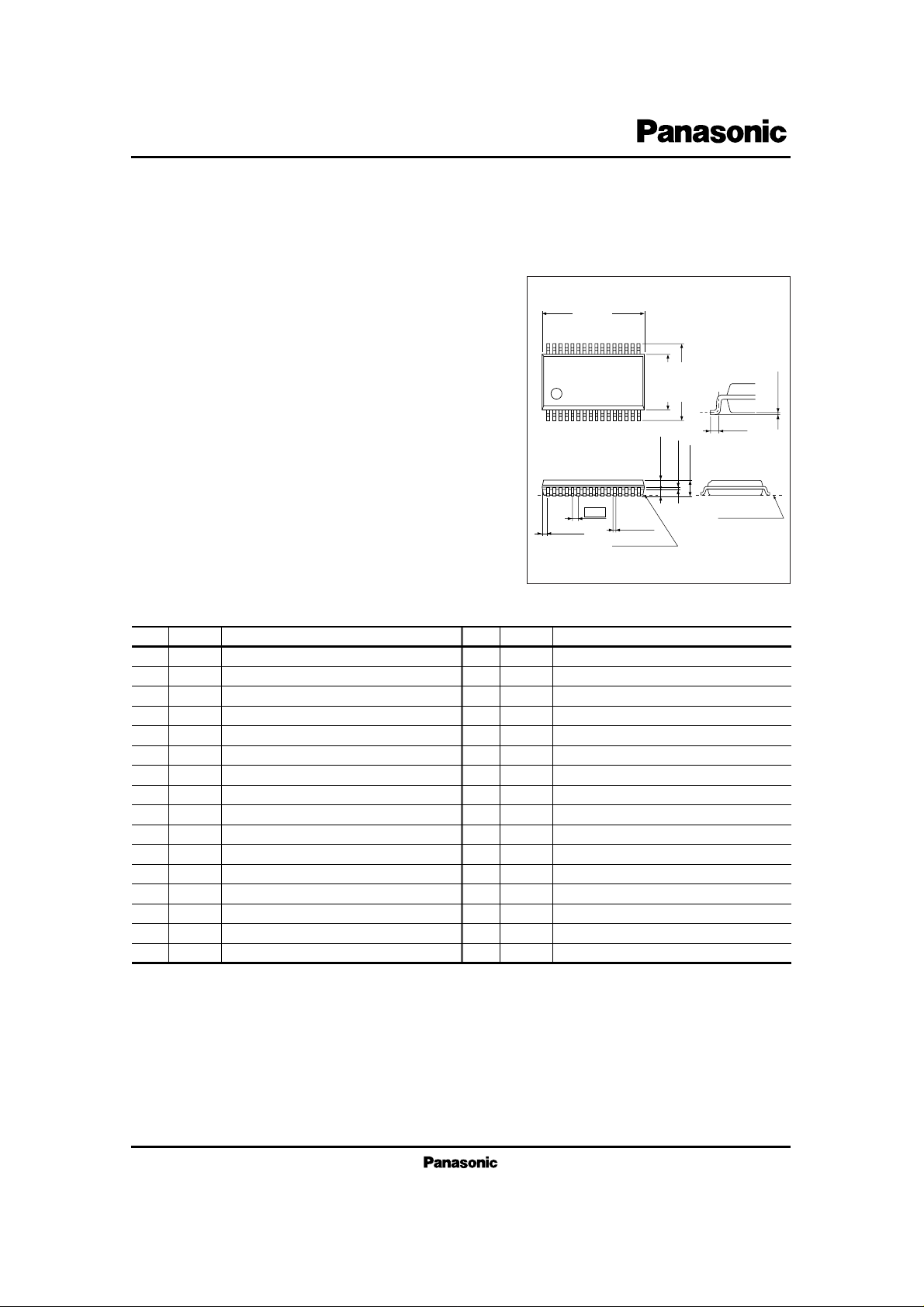
AN3861SA
Sensor-less Motor Drive IC for VTR Movie Cylinder
1.5±0.2
0.65±0.1
0.2
+0.1
– 0.05
116
32 17
Unit : mm
SEATING PLANE
SEATING PLANE
32-pin SSOP Package (SSOP032-P-0300)
11.0±0.3
8.1±0.3
0.1±0.1
(0.5)
(0.625)
0.3
+0.1
– 0.05
0.65
6.1±0.3
■ Pin Descriptions
Pin No.
1
2
3
4
5
6
7
8
9
10
11
12
13
14
15
16
U-phase drive output terminal
U
Drive current output terminal
CS
Switching power supply control output terminal
VSC
W-phase detection terminal
WIN
V-phase detection terminal
VIN
U-phase detection terminal
UIN
Voltage feedback system compensation terminal
PCV
Signal ground
SG
Slope waveform generate terminal (3)
SL3
Slope waveform generate terminal (2)
SL2
Slope waveform generate terminal (1)
SL1
Oscillation terminal
FC
Short brake control terminal
BR
Forward/Reverse change-over terminal
FR
Slope current change-over terminal
HSL
Stand-by input terminal
STB
DescriptionSymbol
Pin No.
17
18
19
20
21
22
23
24
25
26
27
28
29
30
31
32
V
CC
IN2H
OUT2
IN1
IN1
MM
OUT1
Vref
PCI
VS
VB
CS
W
PG
V
PG
–
+
DescriptionSymbol
Power supply terminal
Operational amplifier 2 input terminal
Operational amplifier 2 output terminal
Operational amplifier 1 reverse phase input terminal
Operational amplifier 1 normal phase input terminal
Motor neutral point input terminal
Operational amplifier 1 output terminal
Servo reference voltage input terminal
Current feedback system phase compensation terminal
Motor drive power supply terminal
Unregulated power supply terminal
Drive current output terminal
W-phase drive output terminal
Power ground
V-phase drive output terminal
Power ground
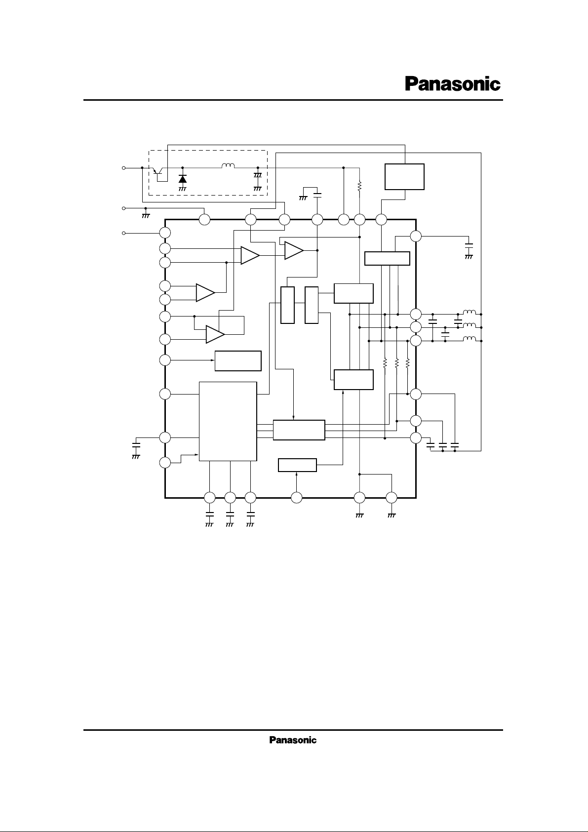
■ Block Diagram
+
–
+
–
+
–
+
–
+
–
0.1µF
0.047µF
0.1µF
0.1µF
0.1µF
A3
0.25Ω
0.022µF × 3
0.022µF0.022µF
0.022µF
8 22 27 26 28 3
7
1
31
29
4
5
6
30 321391011
15
12
14
16
18
19
21
20
23
24
17
Vbatt
V
CC
SW Power Block
SG
MM VB PC1 VS CS
2
VSC (Output for VS Control)
U
V
W
U
IN
V
IN
W
IN
V
S
25
PCV
VCE Detection
Amplifier
Distributor
Source Side
Drive Tr
SW Power
Control
Block
Reference
Power Supply
BEMF Detection
Comparator
Sink Side
Drive Tr
Conducting Phase
Switch Logic
Short Brake
PG PG
BR (High : Brake)
Note) Values of all external C and R are nominal one.
SL 3SL 2SL 1
HSL
560pF
V
ref
OUT 1
OUT 2
IN 1
–
IN 1
+
IN 2
+
STB
(Low : Stand-by)
Forward/Reverse
Control
FR
(High : Forward)
FC
V
CC
V
B
V
S
V
n
I
On
P
D
T
opr
T
stg
V
V
V
V
mA
mW
˚C
˚C
Symbol Rating Unit
6.0
11
11
11
1000
400
–25 to + 70
–55 to + 150
Supply voltage
Unregulated voltage
Motor power supply voltage (under V
B
)
Output terminal voltage
Output current
Power dissipation
Note 1)
Operating ambient temperature
Storage temperature
n=1, 29, 31
n=1, 29, 31
■ Absolute Maximum Rating (Ta=25˚C)
Parameter
Note 1) Package power dissipation when Ta=75˚C
Parameter Symbol Range
■ Recommended Operating Range (Ta=25˚C)
Operating supply voltage
V
CC
V
B
V
S
3.0V to 5.5V
4.0V to 10.5V
1.5V to V
B
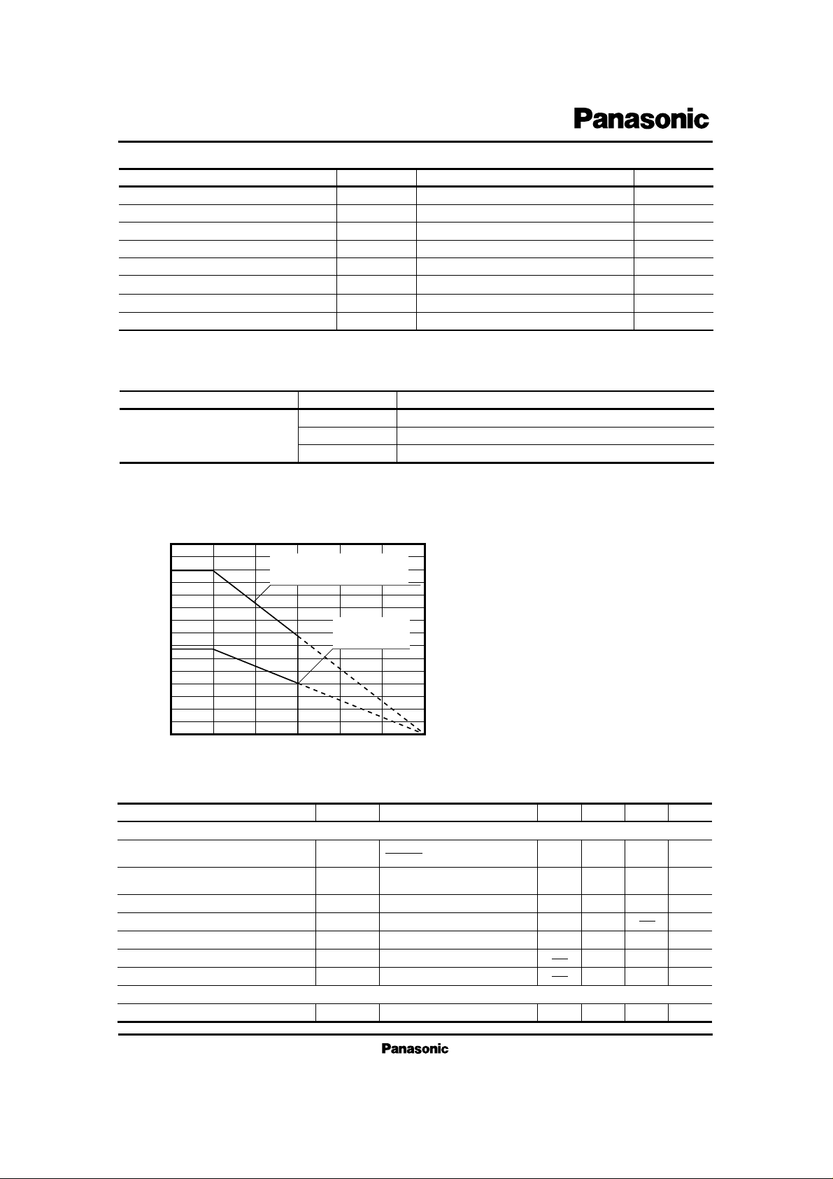
Power Dissipation P
D
(mW)
1400
1200
1000
800
668
600
400
200
0
1290
0 150125100755025
Ambient Temperature Ta (˚C)
Glass epoxy board (50 × 50 × 0.8tmm)
R
thj – a
= 96.9˚C/W
P
D
=1290mW (25˚C)
Single unit
R
thj– a
= 187.1˚C/W
P
D
= 668mW (25˚C)
PD –Ta
■ Package Power Dissipation
Parameter Symbol Condition min typ max
■ Electrical Characteristics (VCC=3.3V, VB=6V, VS=6V, Ta=25±2˚C)
Drive gain Gio 0.170.14
Drive amplifier offset V
iOCS
100 mV
∆OUT1
∆V
CS
Output maximum current
625I
OMAX
mA
Input offset voltage of
V
ref
and OUT1
Brake current
IBR mA
R
CS
=0.25Ω
Sink-side output voltage
V
CE
V0.25
I
O
=100mA
Sink-side saturation voltage
V
SAT (1)
V0.25
I
O
=500mA
Source-side saturation voltage
V
SAT (2)
V0.90
Bemf Detection Block
Drive Block
I
O
=500mA
Comparator hysteresis width
V
HCOM
mV16
875
0.35
0.35
1.3
29
6
750
500
4
0.11
–100
200
0.15
Unit
Operating power supply current
Power Supply Current
I
CC (1)
mA
STB : H
STB power supply current
I
CC (2)
mA
STB : L
Unregulated power supply current (1)
I
BB (1)
µA0.1
V
CC
=0V
Unregulated power supply current (2)
I
BB (2)
mA0.3
V
CC
=3.3V, In
2
+
=0V
15
10
10
1.5
10
6
Parameter Symbol Condition min typ max
■ Electrical Characteristics (cont.) (VCC=3.3V, VB=6V, VS=6V, Ta=25±2˚C)
V
S–U
for VSC=1.6V
when OUT1=V
ref
Oscillator
Slope
Operational Amp. 1 only
Operational Amp. 2 only
Operational Amp. 1 and 2
Mode Switch=HSL, STB, FR, BR
Motor Power Supply Control
22.8
Common-mode input voltage range 0.2V
ICR (1)
V
V
B
–1.4
or V
CC
Input offset current
–50I
IOAI
nA5 50
Input offset voltage
–20V
IOA1, 2
mV–3 20
Output sink current 1– (2)
1.8I
OSI 1 (2)
mA4
Output sink current 2– (2)
2I
OSI 2 (2)
mA4
Output source current (2)
I
OSA 1, 2
mA–15 –2
Input high level
2.0V
SWH
V
Input low level
V
SWL
V0.6
Input bias current
I
BSW
µA25
V
SW
=2V
100
Voltage gain
60G
AI
dB67
Output sink current (1)
20I
OSI1 (1)
µA140
OUT1=0.2V
Common-mode input voltage range
0V
ICR (2)
VVB–1.4
11.0
Input/output gain G
IOS
2.6 Times2.0
∆U
∆V
SC
1.4
Triangular wave oscillation frequency
f
FC
kHz16.3
–14–26
Slope terminal charging current (1)
I
SLC (1)
µA–20
2614
Slope terminal discharging current (1)
I
SLD (1)
µA20
–28–52
Slope terminal charging current (2)
I
SLC (2)
µA–40
5228
Slope terminal discharging current (2)
I
SLD (2)
µA40
–28–52
Slope terminal charging current (3)
I
SLC (3)
µA–40
5228
Slope terminal discharging current (3)
I
SLD (3)
µA40
–42–78
Slope terminal charging current (4)
I
SLC (4)
µA–60
7842
Slope terminal discharging current (4)
I
SLD (4)
µA60
C
FC
=560PF
HSL : L C
FC
=560pF
femf < 160Hz
HSL : L C
FC
=560pF
femf > 181Hz
HSL : H C
FC
=560pF
femf < 160Hz
HSL : H C
FC
=560pF
femf > 181Hz
Unit
Output impedance
12Z
OS
kΩ18 24
Operation point (1)
0.1V
S – U (1)
V0.35 0.6
V
S–U
for VSC=1.6V
when OUT1=Vref + 1
Operation point (2)
0.35V
S – U (2)
V0.63 0.9
Parameter Symbol Condition Reference value
■ Electrical Characteristics [Reference Values] (Ta=25±2˚C)
Thermal protection circuit operation temperature
This is design reference value, and not guaranted one.
T
SD
˚C
V
CC
=3.3V
175
Unit
 Loading...