

Panasonic AN3672NFBP Datasheet
ICs for VCR
AN3672NFBP
Audio signal processor IC for HiFi VCR
incorporating EIAJ sound multiplex system
■ Overview
The AN3672NFBP is a HiFi audio signal processor IC
(NTSC) incorporating EIAJ sound multiplex decoder and
pre/recording amplifier. An adjustment-free sound multiplex decoder is realized through both of f
adjustment of high precision VCO by a reference signal
(f
) and an SIF (4.5 MHz inter-carrier sound intermediate
SC
frequency) signal input.
■ Features
• Built-in EIAJ sound multiplex decoder
• Full adjustment-free by SIF signal input
• f
automatic adjustment of high precision VCO
O
• Built-in pre/recording amplifier
■ Applications
• HiFi VCR
automatic
O
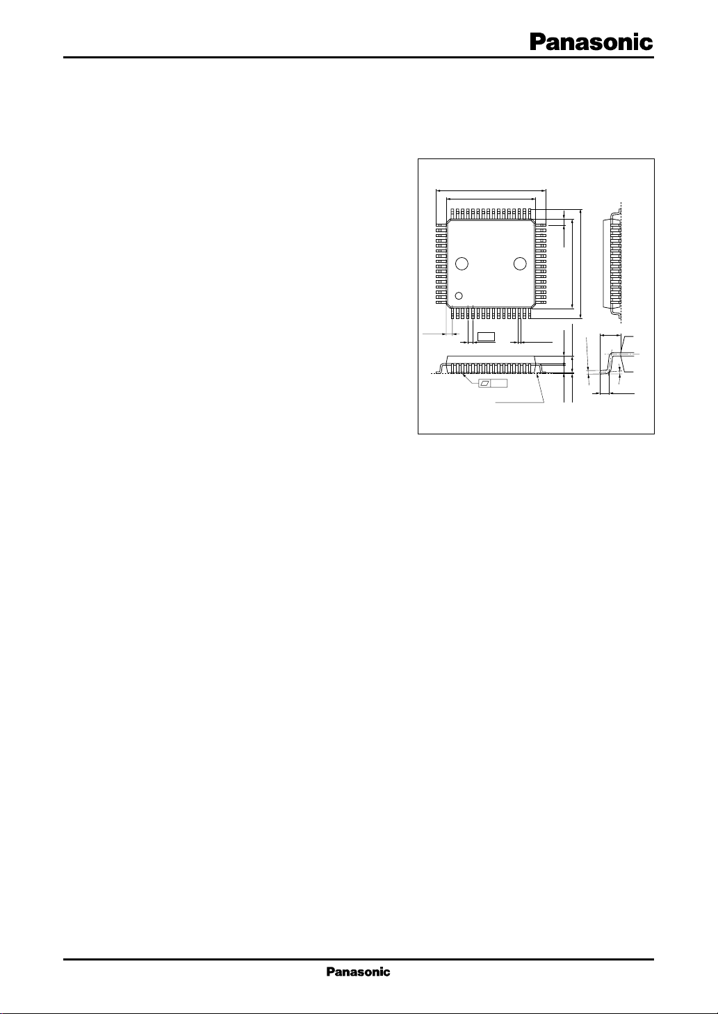
17.2±0.4
14.0±0.3
48 33
49
64
116
(1.00)
0.80
0.10
Seating plane
0.35
+0.10
– 0.05
QFH064-P-1414A
Unit: mm
32
(1.00)
14.0±0.3
17.2±0.4
17
(1.60)
– 0.05
+0.10
1.3±0.11.3±0.1
2.85±0.200.1±0.1
0.20
0° to 10°
(0.80)
1
AN3672NFBP ICs for VCR
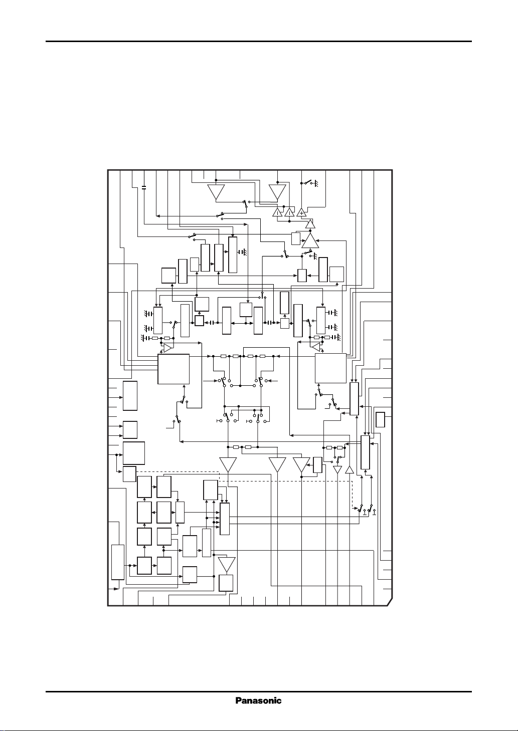
■ Block Diagram
/ BPF monitor)
O
CC
FM in
Noise det./
Rec. AGC det.
CCA out (R)
Forced normal (Normal = L)
common use for ENV-det. output
HA out (f
P/R V
Rec. DC2
Audio FF input
323130292827262524
HEAD1
P/R GND
23
HEAD2
22
COMMON
21
Rec. DC1
20
N.R. REF (L)
CCA out (L)
18
19
N.R. det. 2 (L)
17
N.R. REF (R)
N.R. det. 2 (R)
N.R. det. 1 (R)
Mute CTL
Rec. AGC adj.
GND1 (R)
V
CC1
Logic GND
2
I
C clock
2
C data
I
Logic V
CC
MTS mute CTL
f
SC
(H1 = Mute on)
Main REF
DEM REF
SIF / base band in
HA1
H
SW15
Rec.
PB
R-ch.
VCO
SW12
Rec.LPF
HPF
Liner SW
Noise det.
HOLD timing
33
L
SW11
HA2
Cut amp.
SW14
Det.
Mix.
AGC
SW13
Rec.LPF
L-ch.
VCO
34 16
PB
35
S/H
SW noise
LPF
PC
Audio limit
R-ch.BPF
FM
lim.
SW10
L-ch.BPF
PB LPF
PC
Audio limit
SW4
SW noise
S/H
36
PE
(5 V)
REG
37
38
39
40
41
42
43
44
45
46
47
48
Logic ZZ-PROM
VCO-fOadj.
Mute
CTL
DEM block
50
49
Logic
952 Hz
BPF
AM
demod.
CUE
BPF
4.5fH
trap
51
PNR R-ch.
SW21 SW9
INSW mute
COMP
3.5fH
VCO
Sub
det.
Sub
BPF
52
SW31
Logic
FM
Main
demod.
deem
BS
SW18
From pin 1
R
Mute
SW19
Matrix
Sub deem
LOG
HiFi
Amp.
Output SW
Amp.
amp.
53
Mix.
Normal
L
R
L
54
Mute
Mix.
Normal
L
SW17
55
HiFi
BS
From pin 3
SW16
L
R
Amp.
565758
PNR R-ch.
SW2
SW30
INSW mute
Mix.
L
RFC
Det.
SW22
59
60
61
Input SW (L)
R
63
62
N.R. det. 1 (L)
15
Ext.2-IN (L)
14
Ext.1-IN (L)
13
Sound multiplex output L
12
IN-REF (L)
11
GND1 (L)
10
Ext.2-IN (R)
9
Ext.1-IN (R)
8
Sound multiplex output R
7
IN-REF (R)
6
V
REF
REF1
V
Input SW (R)
L
R
5
CUE det.
4
Ext.3-IN (L)
3
BS-IN (L)
2
Ext.3-IN (R)
1
BS-IN (R)
64
Sub-level det.
(5 V)
Main out
MTS V
DC out
CC
GND2
Line out (R)
LED PORT
(12 V)
CC2
V
Line out (L)
RFC AGC out
Normal out
RFC AGC det.
Comp.
Normal in
Sub REF
(Multi-value output)
2
ICs for VCR AN3672NFBP
■ Pin Descriptions
Pin No. Description
1 BS-IN (R)
2 Ext.3-IN (R)
3 BS-IN (L)
4 Ext.3-IN (L)
5 CUE det.
61/2 V
CC1-VREF
7 IN-REF (R)
8 Sound multiplex output R
9 Ext.1-IN (R)
10 Ext.2-IN (R)
11 GND1 (L)
12 IN-REF (L)
13 Sound multiplex output L
14 Ext.1-IN (L)
15 Ext.2-IN (L)
16 N.R. det. 1 (L-channel: Weighting)
17 N.R. det. 2 (L-channel)
18 N.R. REF (L-channel)
19 CCA out (L)
20 (+) Rec. amp. DCFB pin
21 (+) Rec. amp. output and PB common pin
22 (−) Rec. amp. output and PB-channel 2
input pin
23 Pre/rec.-GND
24 (−) Rec. amp. output and PB-channel 1
input pin
25 Pre/rec.-V
CC
26 (−) Recording amplifier DCFB pin
27 Head switching pulse input for FM audio
28
Envelope detector and forced normal output
29 Pre-amp. output / monitor output
Rec.-mute CTL pin
30 Playback FM input
31 Normal identification noise detection and
rec.-AGC det. pin
Pin No. Description
32 CCA out (R)
33 N.R. REF (R-channel)
34 N.R. det. 2 (R-channel)
35 N.R. det. 1 (R-channel: Weighting)
36 Mute-CTL pin
37 Rec.-AGC adj. pin
38 GND1 (R)
39 PE pin
40 VCC (V
CC1
= 5 V)
41 Logic-GND
42 Serial clock input
43 Serial data input
44 Logic-REG pin
45 Reference signal input pin for fO automatic
adjustment
Sound multiplex mute-CTL pin
46 Main REF
47 DEM REF
48 SIF / base band input
49 Sub level det.
50 Main out
51 MTS VCC (typ. = 5 V)
52 DC out
53 Line out (R-channel)
54 N.C.
55 GND2
56 LED PORT
57 Line out (L-channel)
58 V
(typ. = 12 V)
CC2
59 RFC out
60 RFC-AGC det.
61 Normal out
62 Normal in
63 Comp.
64 Sub REF
3
AN3672NFBP ICs for VCR
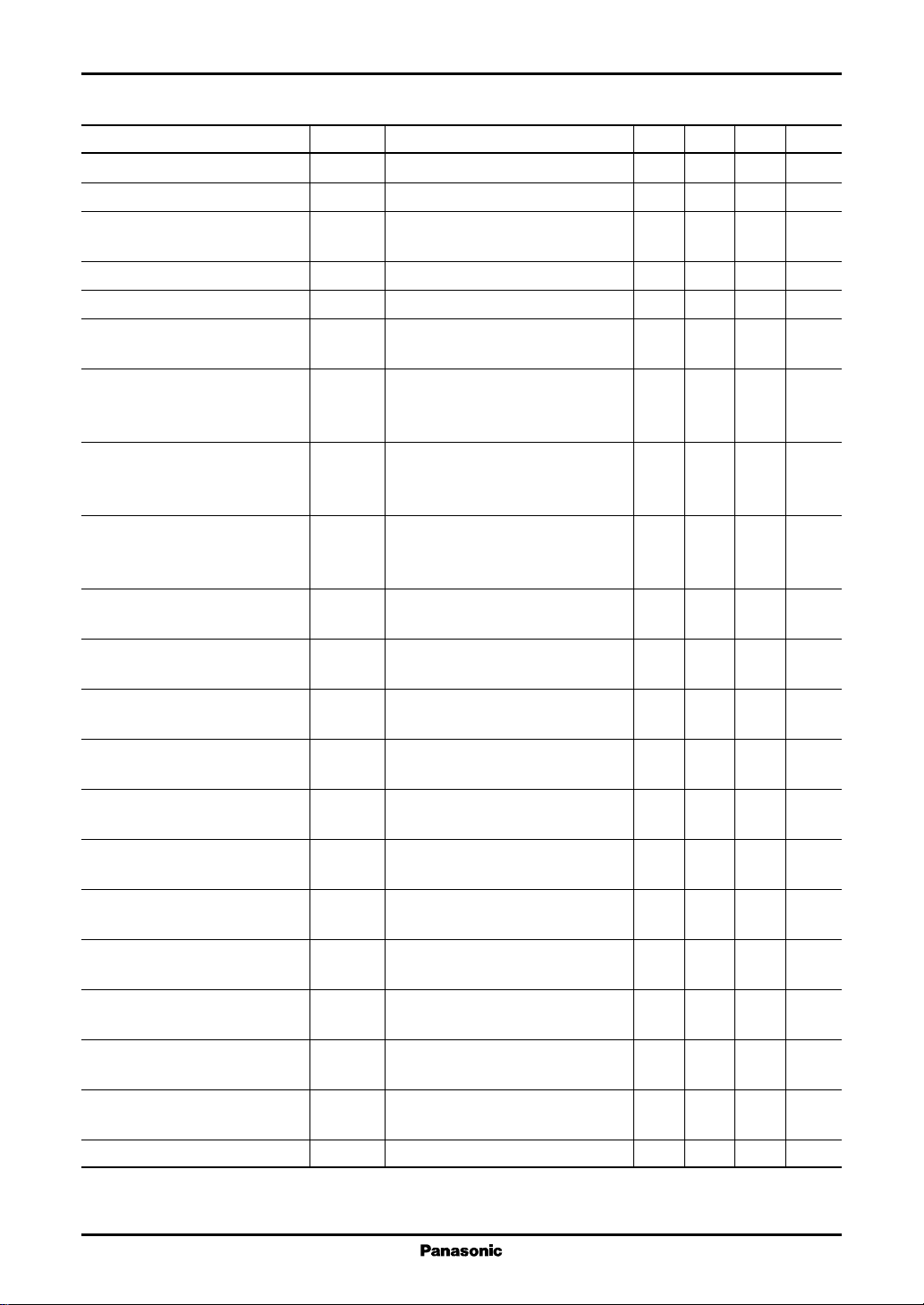
■ Absolute Maximum Ratings
Parameter Symbol Rating Unit
Supply voltage V
1, 2
Power dissipation
Operating ambient temperature
Storage temperature
Note) 1. The reverse insertion of this IC will cause its breakdown.
2. Use this IC paying attention to its surge breakdown. (Refer to "■ Usage Note" in detail.)
3.*1: Except for the power dissipation, operating ambient temperature and storage temperature, all ratings are for Ta = 25°C.
2: The power dissipation shown is the value for Ta = 75°C. (Refer to "■ Application Notes" in detail.)
*
*
1
*
1
*
CC1
V
CC2
P
D
T
opr
T
stg
■ Recommended Operating Range
Parameter Symbol Range Unit
Supply voltage V
CC1
V
CC2
5.5 V
13.0
798 mW
−20 to +75 °C
−55 to +150 °C
4.5 to 5.3 V
8.0 to 12.5
■ Electrical Characteristics at V
= 5 V, V
CC1
= 12 V, Ta = 25°C
CC2
Parameter Symbol Conditions Min Typ Max Unit
Circuit current (5 V) at recording I
Circuit current (12 V) at recording I
Circuit current (5 V) at playback I
Circuit current (12 V) at playback I
CCR1
CCR2
CCP1
CCP2
Recording mode 104 130 156 mA
Measurement after adjusting f
O
Recording mode 5 9 13 mA
Measurement after adjusting f
O
Playback mode 70 95 120 mA
Measurement after adjusting f
O
Playback mode 5 9 13 mA
Measurement after adjusting f
O
ENC out level 1-L VHRO1LVIN = −26.8 dBS, 1 kHz, DIN audio −11.5 −9.5 −7.5 dBS
ENC out level 1-R VHRO1RVIN = −26.8 dBS, 1 kHz, DIN audio −11.5 −9.5 −7.5 dBS
ENC out level 3-L VHRO
3LVIN
= −86.8 dBS, 1 kHz −33 −30 −27 dB
DIN audio, VHRO3L /VHRO
1L
ENC out level 3-R VHRO3RVIN = −86.8 dBS, 1 kHz −33 −30 −27 dB
DIN audio, VHRO3R /VHRO
1R
Normal recording out level VNRO VIN = −26.8 dBS, 1 kHz, Normal out −21.5 −20.0 −18.5 dBS
Line out level L VG2
VIN = −26.8 dBS, 1 kHz −7.5 −6.0 −4.5 dBS
L
Gain = mode (0) Gain = High
Line out level R VG2
VIN = −26.8 dBS, 1 kHz −7.5 −6.0 −4.5 dBS
R
Gain = mode (0) Gain = High
Line out THD L THRMLVIN = −26.8 dBS, 1 kHz 0.05 0.1 %
Line out THD R THRMRVIN = −26.8 dBS, 1 kHz 0.05 0.1 %
Line out V
Line out V
L VMLOLfIN = 1 kHz, at output THD 3% 8.2 10.5 dBS
O-max
R VMLORfIN = 1 kHz, at output THD 3% 8.2 10.5 dBS
O-max
4
ICs for VCR AN3672NFBP
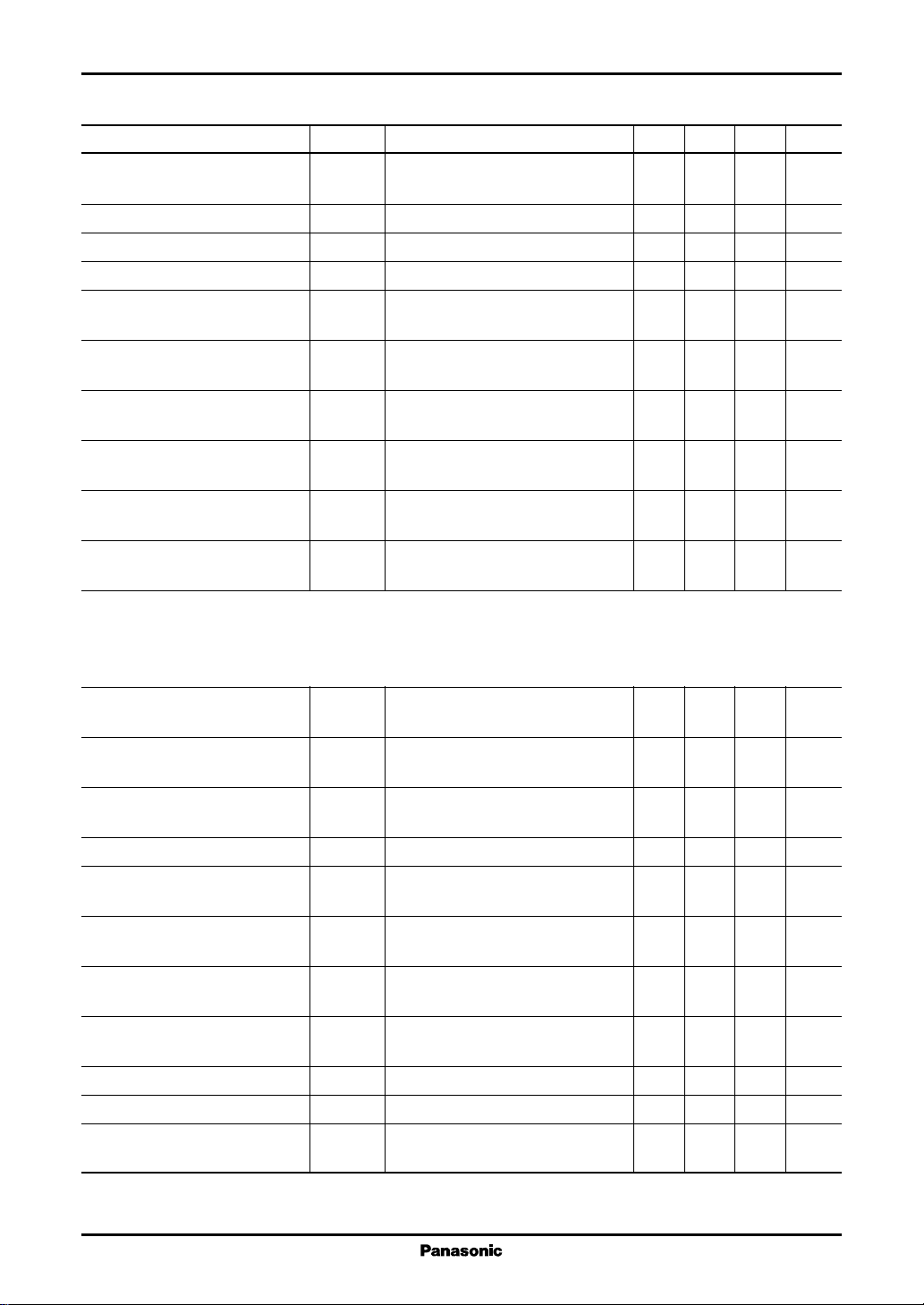
■ Electrical Characteristics at V
= 5 V, V
CC1
= 12 V, Ta = 25°C (continued)
CC2
Parameter Symbol Conditions Min Typ Max Unit
ENC out V
ENC out V
RF conv. out level VRFC V
L VMFELfIN = 1 kHz, at output THD 3% −40.3 dBS
O-max
R VMFERfIN = 1 kHz, at output THD 3% −40.3 dBS
O-max
= −26.8 dBS, 1 kHz −8 −5 −2 dBS
IN
BS monitor mode
Line out S/N L NHLOLRG = 6.8 kΩ, DIN audio 75 80 dB
Line out S/N R NHLORRG = 6.8 kΩ, DIN audio 75 80 dB
1
Crosstalk between inputs 1
*
CT
Ext.1 ∼ Ext.3 in = −16.8 dBS −60 −55 dB
IT
(Select the sound multiplex) 1 kHz, DIN audio
Crosstalk between inputs 2
*
CT
Sound multiplex −75 −65 dB
IE1
1
(Ext.1-IN select) Ext.2 ∼ Ext.3 in = −16.8 dBS
1 kHz, DIN audio
1
Crosstalk between inputs 3
*
CT
Sound multiplex −75 −65 dB
IE2
(Ext.2-IN select) Ext.1, Ext.3 in = −16.8 dBS
1 kHz, DIN audio
1
Crosstalk between inputs 4
*
CT
Sound multiplex −75 −65 dB
IE3
(Ext.3-IN select) Ext.1, Ext.2 in = −16.8 dBS
1 kHz, DIN audio
Crosstalk between channels R→L
CT
Ext.1 in R-ch. = −16.8 dBS, 1 kHz −80 −65 dB
TRL
1
*
DIN audio
1
Crosstalk between channels L→R
*
CT
Ext.1 in L-ch. = −16.8 dBS, 1 kHz −80 −65 dB
TLR
DIN audio
1
Crosstalk between output mode 1
*
CT
HiFi, BS in = −16.8 dBS −75 −60 dB
HN
(Normal select) 1 kHz, DIN audio
Crosstalk between output mode 2
CT
HiFi, BS in = −16.8 dBS −75 −60 dB
NH
1
*
(HiFi select) 1 kHz, DIN audio
1
Crosstalk between output mode 3
*
CT
HiFi, NOR in = −16.8 dBS −60 −55 dB
NH
(BS monitor mode) 1 kHz, DIN audio
Crosstalk between ENC out CT
Ext.1 in R-ch. = −16.8 dBS, 1 kHz −40 −30 dB
ENRL
channels (R→L) DIN audio
Crosstalk between ENC out CT
Ext.1 in L-ch. = −16.8 dBS, 1 kHz −40 −30 dB
ENLR
channels (L→R) DIN audio
1
Output muting ratio L
*
MuteLTV in = −16.8 dBS, 1 kHz, Gain = 1 −60 −45 dB
DIN audio
1
Output muting ratio R
*
Mute
TV in = −16.8 dBS, 1 kHz, Gain = 1 −60 −45 dB
R
DIN audio
VCO output frequency L f
NTSC mode, non-modulation, 1 292 1 300 1 308 kHz
NL
(NTSC) after adjustment
VCO output frequency R f
NTSC mode, non-modulation, 1 692 1 700 1 708 kHz
NR
(NTSC) after adjustment
VCO output L/R mix. ratio L FNLN NTSC mode, mode = (0, 1) 8.5 10 11.5 dB
Note)*1: 10 dB should be reduced from the calculation result because of +10 dB increased input.
5
AN3672NFBP ICs for VCR
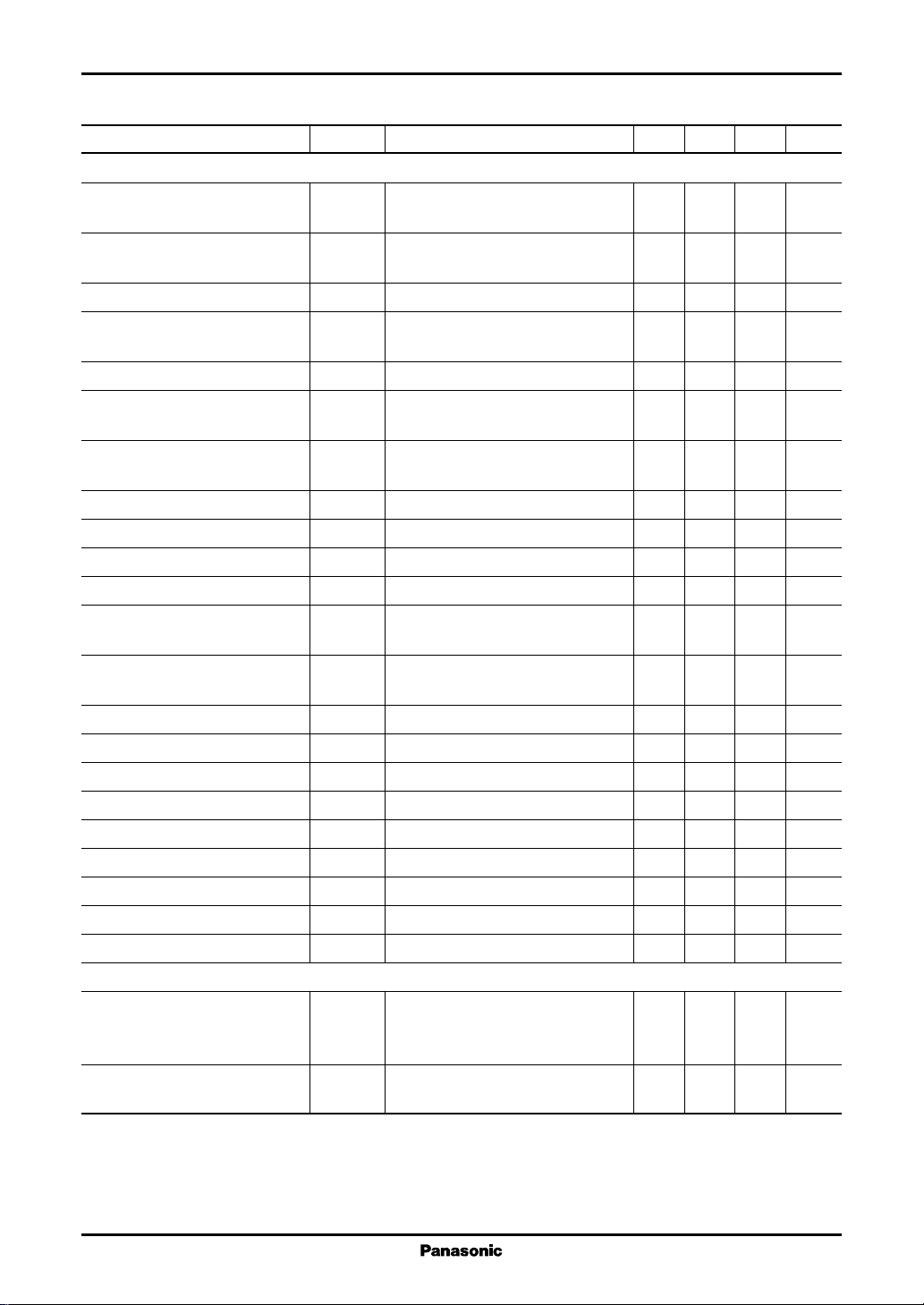
■ Electrical Characteristics at V
= 5 V, V
CC1
= 12 V, Ta = 25°C (continued)
CC2
Parameter Symbol Conditions Min Typ Max Unit
FM deviation L DEV
FM deviation R DEV
FM deviation L/R ratio DEV
VIN = −26.8 dBS, 1 kHz 44 50 56 kHz
L
VIN = −26.8 dBS, 1 kHz 44 50 56 kHz
R
LR
DEVR − DEV
L
−6 0 6 kHz
FM modulation distortion L THFELVIN = −26.8 dBS, 1 kHz, FM RF out 0.5 1.0 %
FM modulation distortion R THFERVIN = −26.8 dBS, 1 kHz, FM RF out 0.5 1.0 %
FM modulation S/N L NHFELRG = 6.8 kΩ, DIN audio, FM RF out 33 40 dB
FM modulation S/N R NHFERRG = 6.8 kΩ, DIN audio, FM RF out 33 40 dB
1.3 MHz BPF frequency BPF11 BPF monitor (L-ch.), f
2
characteristics 1
*
= 1.3 MHz 70 140 210 mV[p-p]
C
1.3 MHz BPF frequency BPF12 fC = 1.45 MHz −10.0 −5.0 2.0 dB
2
characteristics 2
*
1.3 MHz BPF frequency BPF13 fC = 1.15 MHz −4.0 − 0.5 3.0 dB
2
characteristics 3
1.3 MHz BPF frequency BPF15 V
characteristics 5
*
/ V
2
*
(1.05M)
(1.45M)
−13 −1.5 7.0 dB
1.7 MHz BPF frequency BPF21 BPF monitor (R-ch.), NTSC mode 70 140 210 mV[p-p]
2
characteristics 1
1.7 MHz BPF frequency BPF22 f
characteristics 2
*
2
*
fC = 1.7 MHz
= 1.85 MHz −6.0 0 3.5 dB
C
1.7 MHz BPF frequency BPF23 fC = 1.55 MHz −7.0 −1.6 3.0 dB
2
characteristics 3
PB out level 1-L
PB out level 1-R
*
2
*
2
*
VHPO1LVIN = 50 kHz Dev., 1 kHz, Line out −7.5 −6.0 −4.5 dBS
VHPO1RVIN = 50 kHz Dev., 1 kHz, Line out −7.5 −6.0 −4.5 dBS
PB out level L/R ratio BHP −1.5 0 1.5 dB
2
PB out level 3-L
PB out level 3-R
PB out S/N L
PB out S/N R
PB out distortion L
*
2
*
2
*
2
*
2
*
VHPO3LFMIN = 50 kHz −30 dB, DIN audio −66 −60 −54 dB
VHPO3RFMIN = 50 kHz −30 dB, DIN audio −66 −60 −54 dB
NHPOLNon-modulation, Line out, DIN audio
NHPORNon-modulation, Line out, DIN audio
75 80 dB
75 80 dB
THPOLIn: Dev = 100 kHz, f = 1 kHz 0.2 0.8 %
Line out
2
PB out distortion R
*
THPORIn: Dev = 100 kHz, f = 1 kHz 0.2 0.8 %
Line out
Crosstalk between PB out channels
2
*
(R→L)
Crosstalk between PB out channels
2
*
(L→R)
DOC on level DOC1 f
CTP
CTP
VIN = 50 kHz Dev, 1 kHz −80 −65 dB
RL
DIN audio
VIN = 50 kHz Dev, 1 kHz −80 −65 dB
LR
DIN audio
= 1.3 MHz 7 15 30 mV[p-p]
CL
fCR = 1.7 MHz ±50 kHz Dev.
DOC hysteresis DOC2 f
= 1.3 MHz 0.1 1.5 6.0 dB
CL
fCR = 1.7 MHz ±50 kHz Dev.
Note)*2: PB-FM input level: Single 140 mV[p-p], Mix. 280 mV[p-p]
6
ICs for VCR AN3672NFBP
■ Electrical Characteristics at V
= 5 V, V
CC1
= 12 V, Ta = 25°C (continued)
CC2
Parameter Symbol Conditions Min Typ Max Unit
Forced normal on level 1
*
ND1 f = 150 kHz, ND mode = 0, 0 30 75 120 kHz
2
Dev
PB-ch.1 gain G
PB-ch.2 gain G
Gain ratio between PB-channels G
PB-ch.1 input referred noise N
2429
2229
2422
2429
f = 1.5 MHz, 0.2 mV[p-p], AFF = High 70 76 82 dB
f = 1.5 MHz, 0.2 mV[p-p], AFF = L o w 70 76 82 dB
Calculates the G
2429
− G
2229
−30 3dB
Divide by gain after measuring 0.7 1.2 µV[rms]
noise level with 1 MHz BPF
PB-ch.2 input referred noise N
2229
Divide by gain after measuring 0.7 1.2 µV[rms]
noise level with 1 MHz BPF
Rec. output level I
24L
(1.3 MHz component) current output, (R
Rec. output level I
24R
(1.7 MHz component) current output, (R
Rec. output 2nd harmonic distortion I
2fL
(2.6 MHz/1.3 MHz component ratio)
Rec. output 2nd harmonic distortion I
2fR
(3.4 MHz/1.7 MHz component ratio)
Measure the 1.3 MHz component of 6 9 12 mA[p-p]
= 33k), NOR
adj
Measure the 1.7 MHz component of 21 27 33 mA[p-p]
= 33k), NOR
adj
Measure the 2.6 MHz/1.3 MHz −40 −35 dB
component of current output
Measure the 3.4 MHz/1.3 MHz −40 −35 dB
component of current output
Television sound multiplex demodulation block
Note) Input level at 100% modulation Mono, L+R: 106 mV[rms] ( = 0.3 V[p-p])
Sub (L−R) carrier: 63.6 mV[rms] (BIL), 84.8 mV[rms] (Stereo)
Unless otherwise specified, pre-emphasis = off
Mono output level V0(Mon) f = 1 kHz, Mono, 100% modulation, −5.7 −3.7 −1.7 dBS
15 kHz LPF
Mono frequency characteristics V1(Mon) f = 1 kHz, Mono, 100% modulation, −18 −14 −10 dB
(10 kHz) 15 kHz LPF
Mono distortion THD(Mon) f = 1 kHz, Mono, 100% modulation, 0.3 1 %
15 kHz LPF
Mono S/N S/N(Mon) Non-signal, 15 kHz LPF 60 67 dB
Channel balance CB(Mon) f = 1 kHz, Mono, 100% modulation, −10 1dB
15 kHz LPF
Sub output level V0(Sub) f = 1 kHz, BIL, 100% modulation, −5.7 −3.7 −1.7 dBS
15 kHz LPF
Sub frequency characteristics V1(Sub) f = 1 kHz, BIL, 100% modulation, −20 −16 −12 dB
(10 kHz) 15 kHz LPF
Sub distortion THD(Sub) f = 1 kHz, BIL, 100% modulation, 12%
15 kHz LPF
Sub S/N S/N(Sub) Sub carrier + Cue (BIL), 15 kHz LPF 54 60 dB
Sub detection sensitivity SD Sub carrier + Cue (BIL) −9 −4.3 −3dB
Stereo output level V1(st) f = 1 kHz, Stereo, −5.7 −3.7 −1.7 dBS
100% modulation, 15 kHz LPF
Note)*2: PB-FM input level: Single 140 mV[p-p], Mix. 280 mV[p-p] (30-pin)
7
AN3672NFBP ICs for VCR
■ Electrical Characteristics at V
= 5 V, V
CC1
= 12 V, Ta = 25°C (continued)
CC2
Parameter Symbol Conditions Min Typ Max Unit
Television sound multiplex demodulation block (continued)
Stereo separation 1 Sepr f = 1 kHz (L-only), 30 43 dB
100% modulation, 15 kHz LPF
Stereo separation 2 Sepl f = 1 kHz (R-only), 30 43 dB
100% modulation, 15 kHz LPF
Stereo distortion THD(st) f = 1 kHz (Stereo), 100% modulation 0.3 2 %
Stereo S/N Vn(st) Sub carrier 54 60 dB
+ Cue (Stereo) 15 kHz LPF
CUE detection sensitivity CD Sub carrier + Cue (BIL) −11 −6.6 −4dB
Crosstalk (Main→Sub) CT
f = 1 kHz (BIL main), 54 60 dB
MS
100% modulation, 15 kHz LPF
Crosstalk (Sub→Main) CT
f = 1 kHz (BIL sub),
SM
54 60 dB
100% modulation, 15 kHz LPF
Residual carrier (Main) L
Residual carrier (Sub) L
DC offset (Monaural) O
DC offset (Stereo) O
DC offset (Main) O
f = 1 kHz (BIL), 100% modulation 10 20 mV[rms]
CM
f = 1 kHz (BIL), 100% modulation 15 30 mV[rms]
CS
Non-signal 20 100 mV
MO
Sub carrier signal, + Cue signal (Stereo) 20 100 mV
ST
Sub carrier signal 20 100 mV
MA
+ Cue signal (BIL) Main
DC offset (Sub) O
Sub carrier signal 20 100 mV
SB
+ Cue signal (BIL) Sub
Mute attenuation amount (Monaural)
Mute attenuation amount (Stereo) M
Mute attenuation amount (Main) M
Mute attenuation amount (Sub) M
LED-PORT voltage 1 (Mono) LED
LED-PORT voltage 2 (Stereo) LED
LED-PORT voltage 3 (BIL) LED
LOG amp. output 1 V
LOG amp. output 2 V
M
MO
ST
MA
SB
LOG1
LOG2
f = 1 kHz (Mono), 100% modulation 65 80 dB
f = 1 kHz (Stereo), 100% modulation 65 80 dB
f = 1 kHz (BIL), 100% modulation 65 80 dB
f = 1 kHz (BIL), 100% modulation 65 80 dB
Non-signal 0 0.1 0.4 V
1
Sub carrier signal, + Cue signal (Stereo) 1.3 1.6 1.9 V
2
Sub carrier signal, + Cue signal (BIL) 2.7 3.1 4 V
3
f = 440 Hz (Mono), 40% modulation 4 V
f = 440 Hz (Mono), 10% modulation 1V
SIF detection block
Output ratio of SIF to base band VOSIF V
(SIF) = 90 dBµV, fm = 1 kHz − 0.5 0 0.5 dB
i
Mono, 100% modulation,
ratio to VO of base band
SIF total harmonic distortion THDSIF V
(SIF) = 90 dBµV, fm = 1 kHz, 0.3 1.0 %
i
100% modulation
8
ICs for VCR AN3672NFBP
■ Electrical Characteristics at V
= 5 V, V
CC1
= 12 V, Ta = 25°C (continued)
CC2
• Design reference data
Note) The characteristics listed below are theoretical values based on the IC design and are not guaranteed.
Parameter Symbol Conditions Min Typ Max Unit
Data input (high-level) V
Data input (low-level) V
Clock input (high-level) V
Clock input (low-level) V
Mute CTL input (high-level) V
Mute CTL input (low-level) V
HDATA
LDATA
HCLOC
LCLOC
IHMUT
ILMUT
At VCC = 5 V 2.25 5V
At VCC = 5 V 0 0.75 V
At VCC = 5 V 2.25 5V
At VCC = 5 V 0 0.75 V
Mute on 3.5 5V
Mute off 0 1.5 V
Forced normal on level 2 ND2 f = 150 kHz, Mode 01 Dev. 60 kHz
RF conv. AGC level VRFCAG VIN = −16.8 dBS, f = 1 kHz 1.0 dBS
Normal rec. THD TNRO VIN = −26.8 dBS, f = 1 kHz 0.02 %
Normal input crosstalk 1 CTN
Ext.1 in L = −16.8 dBS −75 dB
RR
(Line in R select) DIN audio
Normal input crosstalk 2 CTN
Ext.1 in R = −16.8 dBS −75 dB
LL
(Line in L select) DIN audio
Carrier 3rd harmonics L 3HD
Carrier 3rd harmonics R 3HD
RF recording out −50 dB
L
RF recording out −50 dB
R
1.3 MHz BPF frequency BPF14 1.7 MHz / 1.3 MHz −32 dB
characteristics 4
1.3 MHz BPF frequency BPF16 1.55 MHz / 1.15 MHz −15 dB
characteristics 6
1.7 MHz BPF frequency BPF24 2.1 MHz / 1.7 MHz −13 dB
characteristics 4
1.7 MHz BPF frequency BPF25 1.3 MHz / 1.7 MHz −26 dB
characteristics 5
1.7 MHz BPF frequency BPF26 1.45 MHz / 1385 MHz −8 dB
characteristics 6
BPF group delay difference GDBPF Difference of f
±100 kHz 500 ns
O
(fO ±100 kHz)
VCO fO temperature dependency TVCO fO (T = −10°C) − fO (T = 75°C) 5 kHz
Normal off delay time MON Define with FF timing 3 FF
ENC attack time ENAT f = 5 kHz, VIN = typ.−20 dB 4 ms
ENC recovery time ENRT f = 5 kHz, VIN = typ.−20 dB 65 ms
HOLD pulse width HPUL Test mode, PB 10 µs
ENV out 1 ENV1 1.3 MHz + 1.7 MHz mix. 1.3 V
70 mV[p-p] × 2
ENV out 2 ENV2 1.3 MHz + 1.7 MHz mix. 2.2 V
280 mV[p-p] × 2
HiFi rec. → PB crosstalk CTRP PB, VIN = −16.8 dBS, 1 kHz −79 dB
Dev
9
 Loading...