

ICs for VCR
AN3501NFBP
Luminance, chroma and linear audio signal processing IC for VCR
■ Overview
The AN3501NFBP is a luminance, chroma signal
processing IC for VCR (PAL and NTSC). It also integrates a playback equalizer and an NTSC playback cir-
64
cuit.
A normal audio signal recording/playback circuit is
added so as to design a signal processing PCB in common
for both a HiFi and a normal model, resulting in space
saving of equipment.
This IC is a completely adjustment-free device which
84
has been realized by introducing a adjustment-free technology such as a Zener zap, and contributes to a more
efficient design/development and production of an equipment.
0.6±0.2
■ Features
• Supply voltage range 4.8 V to 5.2 V (600 mW typ.)
• Usable for 4.43 MHz/3.58 MHz systems
• 4.43 MHz system: PAL/NTSC/ME-SECAM
• 3.58 MHz system: NTSC/PAL-N
• Adjustment-free
• Video output level (recording mode)
• Video output level (playback mode)
• White clip level
•f
frequency: sync. tip frequency
O
• FM deviation
• FM level (recording mode)
• Chroma level (recording mode)
• Normal audio circuit built in
• NTSC to PAL conversion by adopting a simplified NTSC playback circuit of a line skip method.
• ME-SECAM discrimination circuit built-in
• All filters built-in, including a CCD filter
• The upper part flicker suppression by adoption of an ACC circuit by the field and an adaptive APC circuit
21.2±0.2
18.0±0.2
63 43
42
18.0±0.2
21.2±0.20.1±0.1
22
121
(1.0)
3.25±0.2
1.55±0.1
0.80
+0.1
0.35
–0.05
Seating plane
+0.1
0.15
–0.05
1.55±0.1
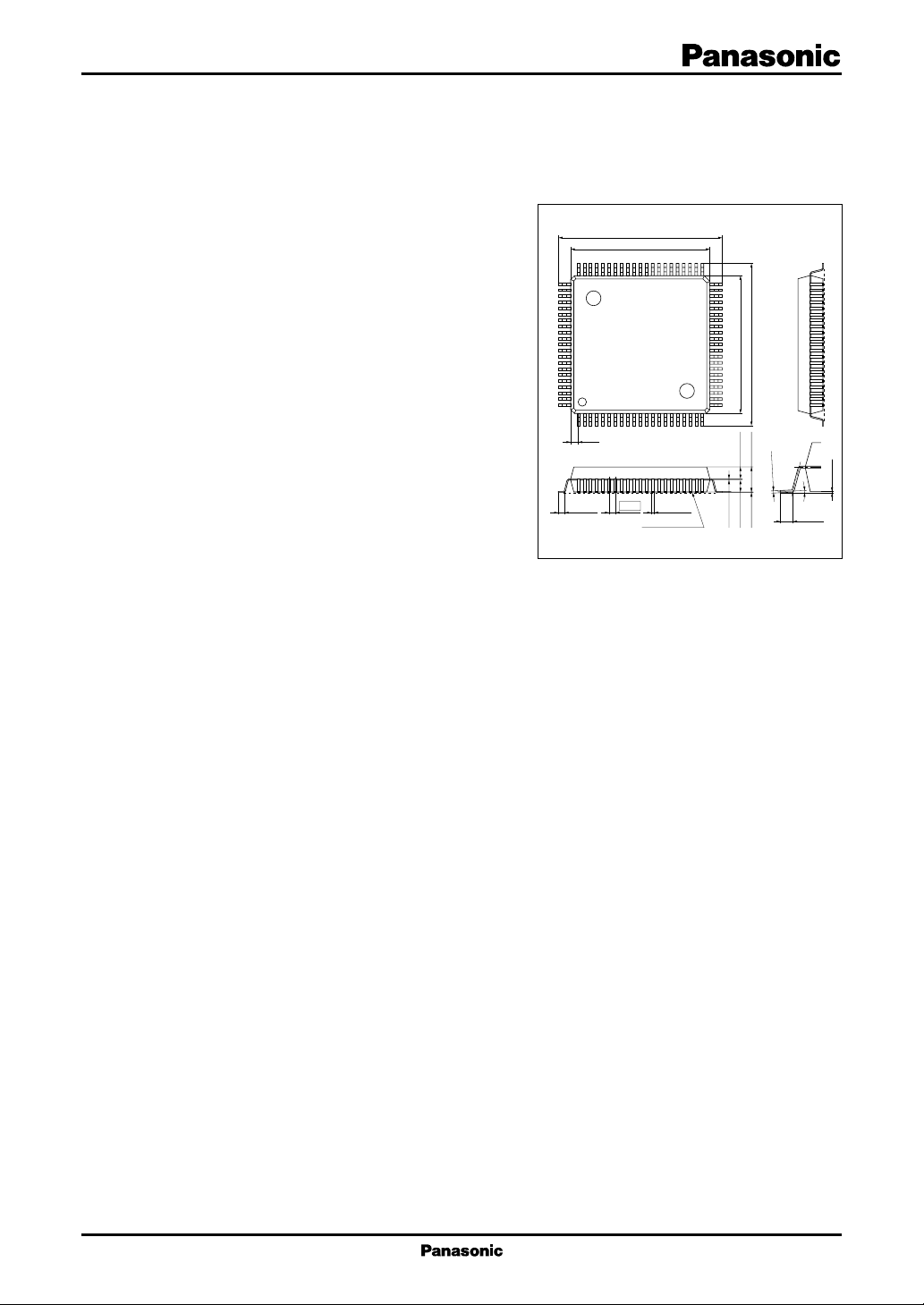
QFH084-P-1818B
Unit: mm
5
0
.0
.1
0
0
–
+
0.15
0° to 10°
0.6±0.2
0.1±0.1
■ Applications
• VCR, camera recorder, combined CTV/VCR set
1
AN3501NFBP ICs for VCR
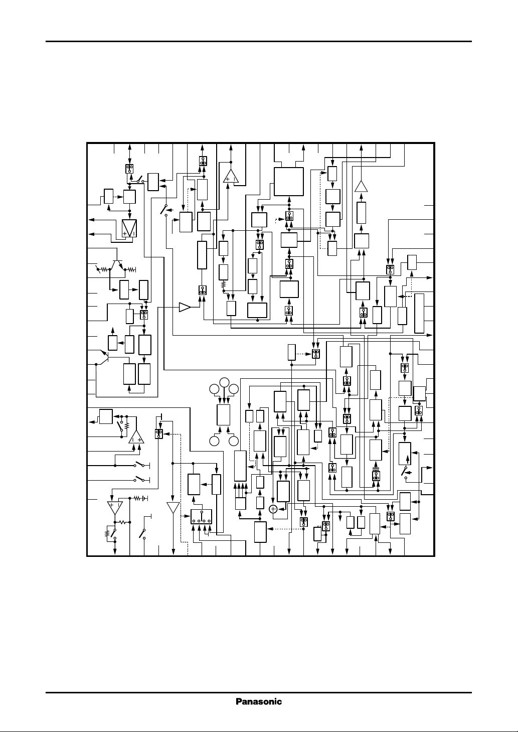
■ Block Diagram
V
(RF)
CC
Rotary SW
M-SECAM/
PAL/NTSC
Ext. RF-in
Through/test2/
PBNTSC
Peaking
4.43 /3.58 SW
6 H/4 H/2 H
GND (NA)
GND (RF)
41
42
VV
RF
Det.
43
44
45
46
47
48
49
50
51
52
53
Trap1
DOP
DO
RF In/Out
SECAM-ID out
40
EE
PB: off
Y/C
AGC
Trap2
Det.
ENV
D-lim.
Line/test1/tuner
Rec. Y
38
39
mix.
CK_off
2fsc
Nor.
37
det.
f
36
Test1
O
VV
FM mod. out
34
35
Nor.
Mod.
clip
W/D
3
HPF
Clamp
Lim.
EE
Main emph. out
32
33
mix.
YNR
EE
HPF
Lim.
N.C.
NLE
NLDE
VV
31
DOP
30
YNR
Nor.
Clamp
VV
Main
VV
54
55
56
Sub
LPF
DEM
50
52
39
57
H
58
f
trap
VV, mute
EE
-on
SLP
-on
LP/SLP-on
66
67
(NA)
CC
V
EE
T
68
69
NA-line out
NA-mute in
AGC
L
Mute
70
NA-tuner in
56
Det.
71
CC
1/2 V
59
SP
-on
60
61
62
63
EE-on
64
65
PB EQ. out
SW
Mode
VV
72
2
Rotary
1/4
73
ID
1/40
BM
Sub
1/4
−1
VCO
74
4.43 on
NA-line in
F det. APC
lock
Side
75
76
GND (VCO)
Art V in
CCD DL out
29
process
Do
1
EE
LPF
EE
Det.
Killer
4phase
VV
77
select
AFC
GND (Y)
28
DP
fH
EE
Det.
78
out
SC
2f
CCD DL in
27
GCA
LPF
CCD
2
Clamp
Det.
Nor.
VV
LP, trick
79
VV
EE
EE
SP
det.
O
To_f
26
LPF
629
BPF
Main
Burst
down
80
Video out
25
Y/C
Clamp
VV
EE
VV
BPF
81
GND (C)
Mute
mix.
4
× 2
EE
VV
24
up
Burst
ACC BM
VXO
82
T
ATT
23
EE
EE
83
L
AGC
SECAM
VV
22
HSS
BPF
CCD
Comb
amp.
PAL
NTSC
PC
H
f
VCO
H
f
84
21
20
19
18
17
Det.
16
15
14
13
SECAM-ID
12
11
10
PAL
det.
ACC
VV
EE, test2
CK_off
V
CC
Tuner in
V
REG
Line in
HSS out
9
8
7
6
5
V
CC
4
V
CC
3
2
EE/VV/trick
1
(Y)
(C)
(C)
ACC out/killer out
2
ICs for VCR AN3501NFBP
■ Pin Descriptions
Pin No. Description
1 Y/C mix. chroma input pin
2 EE/VV/trick changeover
3 PB chroma output
4 Chroma V
5 Chroma V
CC(1)
CC(2)
6 BM DC det.
7 ACC det.
8 F. ACC det. (ROT: high)
9 F. ACC det. (ROT: low)
10 C comb filter input
11 Killer det.
12 C comb filter output
13 SECAM det. 1
14 SECAM det. 2
15 Sync. sepa. det.
16 HSS out
17 AGC det.
18 Line in
19 V
REG
(2.0 V)
20 Tuner in
21 Lumi. V
CC
22 CCD AGC det.
23 Sub clamp det. 1
24 Sub clamp det. 2
25 Video out
26 Sub clamp det. 4
27 CCD DL in
28 Lumi. GND
29 CCD DL out
30 Quasi-sync. pulse input
31 YNR lim. DC
32 N.C. LPF
33 Main emph. FB in/VV edit high
34 Main emph. out
35 Sub clamp det. 3
36 FM mod. out
37 fO det.
Pin No. Description
38 Rec. Y-mix. in
39 Line/test1/tuner changeover
40 SECAM-ID out
41 RF In/Out
42 RF GND
43 RF AGC det./EE edit high
44 Phase shift pos.
45 Phase shift neg.
46 Phase shift in
47 RF V
CC
48 RF EQ. peaking/SQPB high
49 Rotary in
50 M-SECAM/PAL/NTSC changeover
51 Ext. RF in
52 Through/test2/PBNTSC changeover
53 Peaking
54 Main de-emphasis
55 4.43 MHz/3.58 MHz changeover
56 SLP/LP/SP changeover
57 NA-PB amp. in
58 NA-PB EQ. out
59 NA-PB EQ. SW
60 NA-PB NF
61 NA-PB in
62 NA-PB in EQ./SLP
63 NA GND
64 NA-rec. out
65 NA-rec. EQ. NF
66 NA-rec. EQ. LP/SLP
67 NA V
CC
68 NA-line out
69 NA-mute in
70 NA-tuner in
71 1/2 V
CC
72 NA-AGC det.
73 NA-line in
74 VCO f
O
3
AN3501NFBP ICs for VCR
■ Pin Descriptions (cntinued)
Pin No. Description
75 VCO GND
76 ACC out/killer out
77 Rec. AFC/PB APC det.
78 2fSC out
79 Side lock det.
■ Absolute Maximum Ratings
Parameter Symbol Rating Unit
Supply voltage V
Supply current I
2
Power dissipation
Operating ambient temperature
Storage temperature
Note)
1: Except for the operating ambient temperature and storage temperature, all ratings are for Ta = 25°C.
1. *
2: The power dissipation shown is for the IC package at Ta = 70°C
*
*
1
*
1
*
CC
CC
P
D
T
opr
T
stg
Pin No. Description
80 XO/VCXO out
81 C GND
82 XO/VCXO in
83 XO/VCXO out
84 Rec. APC/fH AFC det.
5.5 V
175 mA
660 mW
−20 to +70 °C
−25 to +125 °C
■ Recommended Operating Range
Parameter Symbol Range Unit
Supply voltage V
CC
■ Electrical Characteristics at VCC = 5 V, Ta = 25°C
Parameter Symbol Conditions Min Typ Max Unit
DC characteristics
Supply current (EE) I
Supply current (VV) I
High mode hold voltage V
Middle mode hold voltage V
Low mode hold voltage V
Sync. level insertion mode hold V
voltage
Gray level insertion mode hold V
voltage
Through mode hold voltage V
Rotary SWH hold voltage V
Rotary SWL hold voltage V
4.43 MHz mode hold voltage V
3.58 MHz mode hold voltage V
VCC = 5 V, EE mode 9 2 117 1 44 mA
CCR
VCC = 5 V, VV mode 105 133 164 mA
CCP
Pin 2, pin 39, pin 50, pin 52, pin 56 3.5 5.0 V
H
Pin 2, pin 39, pin 50, pin 52, pin 56 1.75 3.0 V
M
Pin 2, pin 39, pin 50, pin 52, pin 56 0 1.25 V
L
30H
30M
30L
49H
49L
55H
55L
4.8 to 5.2 V
3.5 5.0 V
1.5 3.0 V
0 1.0 V
3.5 5.0 V
0 1.25 V
1.75 5.0 V
0 1.25 V
4
ICs for VCR AN3501NFBP
■ Electrical Characteristics at VCC = 5 V, Ta = 25°C (continued)
Parameter Symbol Conditions Min Typ Max Unit
DC characteristics (continued)
Audio mute hold voltage V
Audio through hold voltage V
After-recording mode hold voltage V
Insertion mode hold voltage V
VV edit mode hold voltage V
EE edit mode hold voltage V
SQPB mode hold voltage V
69H
69L
70H
70L
33H
43H
48H
Luminance recording system
AGC characteristics ∆V
White 100%, − 0.5 0.5 1.0 dB
18-25
VIN = [2.0 V[p-p]]/[0.5 V[p-p]]
EE out amplitude (PAL) V
White 100%, V: S = 7: 3, 1.995 2.1 2.205 V[p-p]
20-25P
VIN = 1 V[p-p]
AGC frequency characteristics f
AGC output level ratio ∆V
EE out amplitude (NTSC) V
20-25fIN
20-25
20-25N
= 5 MHz/1 MHz −2.0 − 0.5 0.5 dB
White 140%, 1.28 V[p-p], 0.05 0.55 1.25 dB
Ratio to V
20-25P
White 100%, V = 0.714 V[p-p], 1.9 2.1 2.3 V[p-p]
VIN = 1 V[p-p]
M LPF frequency characteristics 1 f
18-76(1)
4.43 MHz mode, VIN = 100 mV[p-p] −1.7 0.1 0.9 dB
fIN = 2 MHz/0.15 MHz
M LPF frequency characteristics 2 f
18-76(2)
4.43 MHz mode, VIN = 100 mV[p-p] −4.2 −2.2 −0.7 dB
fIN = 3 MHz/0.15 MHz
M LPF frequency characteristics 3 f
18-76(3)
4.43 MHz mode, VIN = 100 mV[p-p] −35 −30 dB
fIN = 4.43 MHz/0.15 MHz
M LPF frequency characteristics 4 f
18-76(4)
3.58 MHz mode, VIN = 100 mV[p-p] −4.8 −1.8 0.2 dB
fIN = 2.2 MHz/0.15 MHz
M LPF frequency characteristics 5 f
18-76(5)
3.58 MHz mode, VIN = 100 mV[p-p] −39 −27 dB
fIN = 3.58 MHz/0.15 MHz
Sync. separation minimum input S
White 100%, VIN = 0.145 V[p-p], 23 30 37 %
16
sensitivity Pin 76 amplitude
Sync. separation output pulse T
White 100%, VIN = 1.0 V[p-p], 1.14 1.34 1.54 µs
16
front-edge delay including LPF
Sync. separation low-level V
16LRL
(VCC) = 10 kΩ0.7 V
output pulse
Sync. separation high-level V
16HRL
(GND) = 22 kΩ 4.5 V
output pulse
Vertical emph. 1-K value gain 1 G
Vertical emph. 1-K value gain 2 G
76-29(1)V76
76-29(2)V76
Vertical emph. difference signal ∆V
VE
= 400 mV[p-p], LP, fIN = 150 kHz −3.0 −1.5 0 dB
= 400 mV[p-p], LP, fIN = 2 MHz −1.5 0 1.5 dB
White 100%, 1 V[p-p] 30 100 mV[p-p]
amplitude
3.5 5.0 V
0 1.25 V
4.0 5.0 V
0 1.0 V
4.0 5.0 V
4.0 5.0 V
3.25 5.0 V
5
AN3501NFBP ICs for VCR
■ Electrical Characteristics at VCC = 5 V, Ta = 25°C (continued)
Parameter Symbol Conditions Min Typ Max Unit
Luminance recording system (continued)
Vertical emph. X value gain G
CCD input output level V
NL emphasis/detail enhancer G
31-33VIN
29
NE(1)
frequency characteristics 1 fIN = 500 kHz/150 kHz
NL emphasis/detail enhancer G
NE(2)
frequency characteristics 2 fIN = 2 MHz/150 kHz
NL emphasis/detail enhancer G
NE(3)
frequency characteristics 3 fIN = 500 kHz/150 kHz
NL emphasis/detail enhancer G
NE(4)
frequency characteristics 4 fIN = 2 MHz/150 kHz
NL emphasis/detail enhancer G
NE(5)
frequency characteristics 5 fIN = 500 kHz/150 kHz
NL emphasis/detail enhancer G
NE(6)
frequency characteristics 6 fIN = 2 MHz/150 kHz
NL emphasis/detail enhancer G
NE(7)
frequency characteristics 7 fIN = 2 MHz/150 kHz
Main emphasis gain G
Main emphasis standard output V
ME
ME
level
White clip level LV
Dark clip level LV
FM mod. output frequency f
WC
DC
36P
(4.43 PAL) PAL mode
FM mod. output frequency f
36N(1)
(4.43 NTSC) NTSC mode
FM mod. output frequency f
36N(2)
(3.58 NTSC) NTSC mode
FM mod. output secondary 2f
36P
distortion (PAL)
FM mod. deviation (PAL) D
FM mod. deviation (NTSC) D
Rec. FM total output amplitude V
36P
36N
FM
(PAL)
Rec. FM amp. f
38-41
frequency characteristics
Luminance playback system
FM demodulation sensitivity ∆V
53V
(VHS)
FM demodulation sensitivity ∆V
53S
(SQPB)
= 40 mV[p-p], fIN = 150 kHz −18.5 −15.0 −11.5 dB
VIN = 1 V[p-p], white 100% 375 405 4 4 0 mV[p-p]
SP/edit: V76 = −20 dB, 0.4 1.2 2.0 dB
SP/edit: V76 = −20 dB, 1.7 2.9 4.1 dB
SP/normal: V76 = −20 dB, 1.1 2.1 3.1 dB
SP/normal: V76 = −20 dB, 3.2 4.7 6.2 dB
LP: V76 = −20 dB, 2.54 3.84 5.14 dB
LP: V76 = −20 dB, 3.9 5.9 7.9 dB
LP: V76 = 0 dB, 0.2 0.9 1.6 dB
1 kΩ/220+0.1 µF, fIN = 150 kHz 13 15 17 dB
White 100%, 1 V[p-p] 350 400 450 mV[p-p]
White 100% 176 183 190 %
White 100% 43 55 65 %
No input 4.43 MHz mode, 3.75 3.81 3.85 MHz
No input 4.43 MHz mode, 3.37 3.47 3.57 MHz
No input 3.58 MHz mode, 3.29 3.39 3.49 MHz
No input PAL mode −45 −35 dB
White 100% 0.95 1.0 1.05 MHz
White 100% 0.9 1.0 1.1 MHz
V36 /4 × G
, V36: pin 36 amplitude 332.5 350 367.5 mV[p-p]
38-41
10 MHz/4 MHz −2.5 − 0.5 0.5 dB
Pin 51 input, fIN = 3.8 MHz, 4.8 MHz 0.13 0.175 0.22 V/MHz
Pin 51 input, fIN = 5.4 MHz, 7.0 MHz 0.13 0.175 0.22 V/MHz
6
ICs for VCR AN3501NFBP
■ Electrical Characteristics at VCC = 5 V, Ta = 25°C (continued)
Parameter Symbol Conditions Min Typ Max Unit
Luminance playback system (continued)
PB output amplitude V
Drop out detect SW on level S
Drop out detect hysteresis ∆S51f
Env. detect SW operating time T
NL de-emphasis G
frequency characteristics 1 f
NL de-emphasis G
frequency characteristics 2
NL de-emphasis G
frequency characteristics 3 f
NL de-emphasis G
frequency characteristics 4
NL de-emphasis G
frequency characteristics 5
YNR 1-K value gain EDNC G
YNR 1-K value gain VNC G
YNR difference element ∆V
amplitude EDNC
YNR difference element ∆V
amplitude VNC
YNR X value gain EDNC G
YNR X value gain VNC G
YNR lim. (VNC) output level 1 V
YNR lim. (VNC) output level 2 V
YNR lim. (VNC) output level 3 V
CCD AGC cover range ∆V
Noise cancellar G
frequency characteristics 1 CCD LPF, f
Noise cancellar G
frequency characteristics 2 CCD LPF, f
Noise cancellar G
frequency characteristics 3 CCD LPF, f
Noise cancellar G
frequency characteristics 4 CCD LPF, f
Video output sync. DC level ∆V
Video output quasi-V offset voltage
Video output quasi-H offset voltage
∆V
∆V
Pin 51 input, f
PB
51fIN
IN
AM wave 1 kHz, V
ENV
f
IN
SP: V
ND(1)
IN
SP: V
ND(2)
LP: V
ND(3)
IN
LP: V
ND(4)
LP: V
ND(5)
White 100%, V
54-29E
White 100%, V
54-29V
Rectangular wave, V
EDNC
Rectangular wave, V
VNC
31-25EVIN
31-25VVIN
25YL(1)VIN
25YL(2)VIN
25YL(3)VIN
31V54
CCD Gain ±3 dB
Normal mode, V
25N(1)
Normal mode, V
25N(2)
Normal mode, V
25N(3)
Edit mode, V
25N(4)
White 100%, V
SYNC
25AV30
25GV30
= 3.8 MHz, 4.8 MHz 1.995 2.1 2.205 V[p-p]
IN
= 4 MHz, 0 dB = 350 mV[p-p] −22 −18 −14 dB
= 4 MHz, 0 dB = 350 mV[p-p] 1.0 3.0 5.0 dB
= 350 mV, 180 224 270 µs
IN
= 4 MHz
= −20 dB, −2.7 −1.7 − 0.7 dB
IN
= 500 kHz/150 kHz
= −20 dB, 2 MHz/150 kHz −5.5 −4.2 −3.0 dB
IN
= −20 dB, −6.2 −3.9 −2.2 dB
IN
= 500 kHz/150 kHz
= −20 dB, 2 MHz/150 kHz −9.0 −7.5 −6.2 dB
IN
= 0 dB, 2 MHz/150 kHz −2.7 −2.0 −1.3 dB
IN
= 160 mV[p-p] 4.5 6.0 7.5 dB
IN
= 160 mV[p-p] 1.8 3.3 4.8 dB
IN
= 160 mV[p-p] 30 100 mV[p-p]
IN
= 160 mV[p-p] 10 100 mV[p-p]
IN
= 40 mV[p-p], f
= 40 mV[p-p], f
= 800 mV[p-p], f
= 300 mV[p-p], f
= 100 mV[p-p], f
= 150 kHz −4.9 −2.9 −1.3 dB
IN
= 150 kHz 0.6 2.1 3.6 dB
IN
= 150 kHz 26 40 5 3 mV[p-p]
IN
= 150 kHz 13.5 25.0 37.0 mV[p-p]
IN
= 150 kHz 80 110 1 40 mV[p-p]
IN
= 160 mV[p-p], rectangular wave, 0 30 100 mV[p-p]
= −30 dB, Including −13.0 −8.0 −4.8 dB
27
= 1 MHz/150 kHz
IN
= −30 dB, Including −9.3 −4.5 −2.3 dB
27
= 2 MHz/150 kHz
IN
= 0 dB, Including − 0.8 1.2 2.7 dB
27
= 2 MHz/150 kHz
IN
= −30 dB, Including − 0.3 −1.0 0.5 dB
27
= 2 MHz/150 kHz
IN
= 317 mV[p-p] 0.8 0.95 1.1 V
27
= 5 V −30 0 60 mV
= 2.5 V 0.85 1.0 1.15 V
7
AN3501NFBP ICs for VCR
■ Electrical Characteristics at VCC = 5 V, Ta = 25°C (continued)
Parameter Symbol Conditions Min Typ Max Unit
Luminance playback system (continued)
Chroma mix. output gain G
Chroma mix. frequency characteristics
RF-AGC output amplitude V
RF-AGC sensitivity S
RF-AGC output distortion D
RF-AGC maximum gain G
RF-EQ. frequency characteristics
RF-EQ. frequency characteristics
RF-EQ. frequency characteristics
RF-EQ. frequency characteristics
RF-EQ. total characteristics V
1-25VIN
f
1-25
41-45VIN
RF
RF
RFAGCVIN
2 GEQ2 VIN = 20 mV[p-p], f = 1 MHz/5 MHz −24.0 −15.0 −9.0 dB
3 GEQ3 f = 2 MHz/5 MHz −9.8 −5.3 −3.3 dB
4 GEQ4 f = 630 kHz/5 MHz −30 −15 dB
5 GEQ5 f = 8 MHz/5 MHz −30 −15 dB
41-36VIN
Chroma recording system
Output DC for color V
Output DC for killer V
Burst up gain G
Rec. APC pull in range 1 f
Rec. APC pull in range 2 f
Rec. APC pull in range 3 f
Rec. APC pull in range 4 f
VXO free-run frequency 1 f
VXO free-run frequency 2 f
Rec. chroma output amplitude V
ACC characteristics 1 ∆V
ACC characteristics 2 ∆V
630k LPF f
76CO
76CK
BUPVIN
APC(1)
APC(2)
APC(3)
APC(4)
VXO(1)
VXO(2)
CR
ACC1VIN
ACC2VIN
RL(1)
frequency characteristics 1 150 kHz/630 kHz
630k LPF f
RL(2)
frequency characteristics 2 3 MHz/630 kHz
630k LPF f
RL(3)
frequency characteristics 3 4.43 MHz/630 kHz
630k LPF group delay GD
630k LPF f
RL
RL(4)
frequency characteristics 4 2 MHz/630 kHz
SECAM discrimination output DC 1
SECAM discrimination output DC 2
V
40(1)
V
40(2)
= 600 mV[p-p], fIN = 5 MHz 4.9 6.6 8.3 dB
VIN = 600 mV[p-p], fIN = 5 MHz/1 MHz
− 0.5 0.3 1.0 dB
= 200 mV[p-p], f = 4 MHz 17 0 215 265 mV[p-p]
±6 dB input 0.5 3.0 dB
VIN = 400 mV[p-p], f = 4 MHz −44 −35 dB
= 20 mV[p-p], f = 4 MHz 8.5 10.5 12.5 dB
= 200 mV[p-p] 305 435 605 mV[p-p]
Color, V11 = 3.5 V 3.5 V
Killer, V11 = 1.5 V 0.5 V
= 1: 1 (B = 300 mV[p-p]) 5 6 7 dB
4.43 MHz mode, fIN = fSC +500 Hz 500 800 Hz
4.43 MHz mode, fIN = fSC −500 Hz −800 −500 Hz
3.58 MHz mode, fIN = fSC +500 Hz 500 800 Hz
3.58 MHz mode, fIN = fSC −500 Hz −800 −500 Hz
4.43 MHz mode, SECAM mode −100 0 1 00 Hz
3.58 MHz mode, SECAM mode −100 0 1 00 Hz
B: C = 1: 2 chroma level 75.6 82 88.4 mV[p-p]
= 1: 1, +9, −5 dB, V49 = 5 V 3dB
= 1: 1, +9, −5 dB, V49 = 0 V 3dB
4.43 MHz mode, VIN = 200 mV[p-p], − 0.7 0.3 1.3 dB
4.43 MHz mode, VIN = 200 mV[p-p], −25 −15 dB
4.43 MHz mode, VIN = 200 mV[p-p], −35 −20 dB
4.43 MHz mode, VIN = 200 mV[p-p], 310 360 4 10 ns
fIN = 630 kHz
3.58 MHz mode, VIN = 200 mV[p-p], −2.0 0 2.0 dB
4.43 MHz mode, PAL mode, fIN = 4.43 MHz
0 0.65 V
4.43 MHz mode, SECAM mode, 4 5V
fIN = 4.25 MHz, 4.41 MHz
8
 Loading...