

Panasonic AN3328S Datasheet
ICs for VCR
AN3328S
2-head recording and playback amplifier IC (A2) for HiFi VCR
■ Overview
The AN3328S is a 2-head recording and playback amplifier IC for HiFi audio, and realized
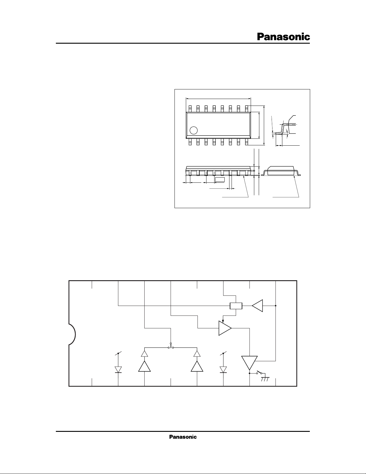
reduction of pin numbers. The package is a small
outline of 16 pins, 1.27 mm pitch and supply voltage is 5 V of single supply.
■ Features
• Damping-less amp. in playback system
• No adjustment of recording current by AGC
• 3-step switchover of recording current level with
the current emphasis switch (typ. ± 1.8 dB)
■ Applications
• HiFi VCR
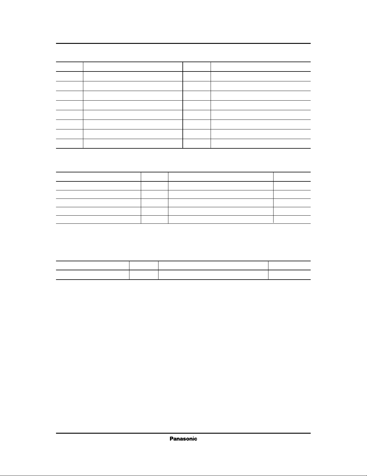
■ Block Diagram
−0.05
+0.10
0.15
Seating plane
Unit: mm
0° to 10°
0.50 ± 0.20
10.09 ± 0.20
16 9
4.30 ± 0.20
6.40 ± 0.30
18
0.65 ± 0.100.65 ± 0.10
1.50 ± 0.200.10 ± 0.10
(0.60)
1.27
0.40 ± 0.10
Seating plane
SOP016-P-0225C
REC / PB selectHSW
16
1
REC C
15
2
REC reg1
PB out &
REC / mute
14
HA1 HA2
3
CH1 in
REC in
13
LH
4
GND (small signal)
GND
12
5
CH2 in
11
AGC
6
REC reg2
Det
V
10
Curr.
Amp.
7
REC out
CC
REC curr. monitor
9
8
Curr. emph. SW
1
AN3328S ICs for V CR
■ Pin Descriptions
Pin No. Description
1 Audio head SW
2 REC regulator1
3 Head amp. input ch.1
4 GND (small signal)
5 Head amp. input ch.2
6 REC regulator2
7 REC out
8 Curr. emph. SW
Pin No. Description
9 REC curr. monitor (control)
10 V
CC
11 REC AGC det
12 GND
13 REC input
14 PB out & REC / mute SW
15 REC C
16 REC/PB select SW
■ Absolute Maximum Ratings
Parameter Symbol Rating Unit
Supply voltage V
Supply current I
Power dissipation
Operating ambient temperature
Storage temperature
Note)*1: Except for the operating ambient temperature and storage temperature, all ratings are for Ta = 25°C.
2: The power dissipation shown is for the IC package in free air at Ta = 70°C.
*
*2
*1
*1
CC
CC
P
D
T
opr
T
stg
6V
mA
240 mW
-20 to +70 °C
-55 to +125 °C
■ Recommended Operating Range
Parameter Symbol Range Unit
Supply voltage V
CC
4.5 to 5.5 V
2
ICs for VCR AN3328S
■ Electrical Characteristics at Ta = 25°C
Parameter Symbol Conditions Min Typ Max Unit
REC I
10(REC)
Circuit current REC / PB SW: High
REC I
AGC level REC / PB SW: High
REC DI
AGC control characteristics REC / PB SW: High
REC Recording current D
2nd harmonic distortion VIN = 260 mV[p-p], 2 MHz
REC V
Mode hold voltage VIN = 260 mV[p-p], 2 MHz
REC V
Over REC hold voltage REC / PB SW: High
REC V
Normal hold voltage REC / PB SW: High
REC V
S-VHS hold voltage REC / PB SW: High
REC I
7L
Over REC current ratio REC / PB SW: High
REC I
7H
S-VHS current ratio REC / PB SW: High
REC V
14H(REC)VCC
Mute hold voltage 1 REC / PB SW: High
REC V
14L(REC)VCC
Mute hold voltage 2 REC / PB SW: High
PB I
10(PB)
Circuit current REC / PB SW: Low
PB G
CH1 gain HSW: High, VIN = 0.1 mV[p-p], 2 MHz
PB G
CH2 gain HSW: Low, VIN = 0.1 mV[p-p], 2 MHz
PB DG
CH1 1.5 M / 2 M gain ratio HSW: High, VIN = 0.1 mV[p-p], 2 MHz
PB DG
CH2 1.5 M / 2 M gain ratio HSW: Low, VIN = 0.1 mV[p-p], 2 MHz
PB G
3-14
CH1 / CH2 gain ratio G
Noise referred to PB N
CH1 input REC / PB SW: Low HSW: High
Noise referred to PB N
CH2 input REC / PB SW: Low HSW: Low
Note) The typical value in the parenthesis is not the guaranteed one.
VCC = 5.0 V 56 (66) 76 mA
V
7
7
7
16H
8L
8M
8H
= 5.0 V 44 (48) 52
CC
VCC = 5.0 V (0.2) 1.0 dB
VCC = 5.0 V, REC / PB SW: High (−43) −35 dB
VCC = 5.0 V, REC / Mute SW: Low 3.6 Vcc V
VCC = 5.0 V 0 1.2 V
VCC = 5.0 V 1.8 3.2 V
VCC = 5.0 V 3.8 Vcc V
mA[p-p]
→ I7VCC = 5.0 V 1.3 (1.8) 2.3 dB
→ I7VCC = 5.0 V −2.3 (−1.8) −1.3 dB
= 5.0 V 3.6 Vcc V
= 5.0 V 0 1.4 V
VCC = 5.0 V 9 (13) 17 mA
VCC = 5.0 V, REC / PB SW: Low 72 (76) 80 dB
3-14
VCC = 5.0 V, REC / PB SW : Low 72 (76) 80 dB
5-14
VCC = 5.0 V, REC / PB SW: Low 0 (0.5) 1 dB
3-14
VCC = 5.0 V, REC / PB SW: Low 0 (0.5) 1 dB
5-14
→ VCC = 5.0 V, REC / PB SW: Low −20 2dB
5-14VIN
3-14
5-14
= 0.1 mV[p-p], 2 MHz
VCC = 5.0 V 1.0
VCC = 5.0 V 1.0
mV[rms]
mV[rms]
3
 Loading...