

Panasonic AN3275SB Datasheet
ICs for VCR
AN3275SB
CM detection IC for VCRs in the North American market
■ Overview
The AN3275SB is an IC which detects both a low
luminance of video signal and a low sound amplitude
based on
that is ADLE Inc.'s
patent of the CM detection technology. Using this IC and
a free memory area in a microcomputer, you can easily
carry out a CM detection for VCRs used in the North
America.
■ Features
• Video black detection
• Low sound detection
• Generation of various masking pulses
(Detecting H-mask, V-mask and envelope)
• Generation of the pulse (CLR pulse) for an event latch
• Usable for COMMERCIAL ADVANCE, MOVIE AD-
VANCE and CA-LITE
■ Applications
• Stand-alone VCR
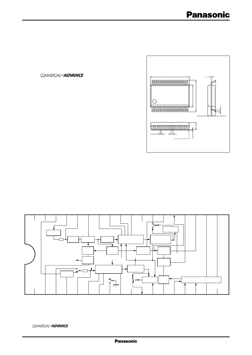
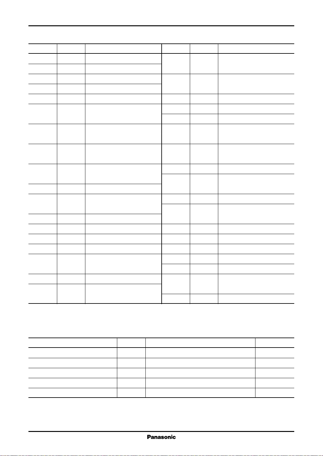
■ Block Diagram
Unit: mm
+0.10
15.2±0.3
36 19
8.4±0.3
118
0.3±0.11 0.8
Seating plane
0.1±0.1
–0.05
0.2
11.93±0.3
1.30±0.25 1.30±0.25
2.85±0.2
SSOP036-P-0450A
0.5
GND36CA/MA SEL
35
Clamp
1
2
CC
V
HMW
V IN33C TRAP32CL CAP31CA V FIL30CA V LEV29MA V FIL28MA V LEV27N.C.26V DET25SYNC FIL24VS OUT23VMW22VMD21ENVH DET20ENVL DET
34
MA
3
RA IN
H mask
Amp. 2
4
PA IN
LPF
5
Clamp
MM3
H-DL
MM4
H-WD
LPF3
6
MA V LEV
Amp.
BP
Non-audio
7
MA A FIL
Sync.
sepa.
V mask
detect
CA
8
MA
CA A FIL
Black video
detect
H mask
CA
9
CA A LEV
V-sync.
E/V mask
Audio 1
Latch 2
MA
10
CA
sepa.
Counter
E/V mask
11
A DET
Video 1
Latch 2
MM2
V-WID
12
CLR IN
Counter
MM1
V-DL
V mask
Mix.
13
CLR OUT
E/V mask
ENV mask
14
ENV DET
ENV detector
15
16
PB FM IN
17
HSW IN
ENV ADJ.
19
18
Note) is a trademark registered by SRT, Inc., invented by Jerry Iggulden who closed a licensing contract under
the cooperation of Arthur D. Little Enterprises, Inc.
1
AN3275SB ICs for V CR
■ Pin Descriptions
Pin No. Symbol Description
1VCCSupply voltage (5 V typ.)
2 HMW
H-mask width period adjustment
3 RA IN Audio recording input
4 PA IN Audio playback input
5 A FIL Audio filter
6
MA A LEV
MOVIE ADVANCE audio
detection level adjustment
Pin No. Symbol Description
19
ENV L DET
PB FM envelope peak
detection (below)
20
ENV H DET
PB FM envelope peak
detection (upper)
21 VMD V-mask time delay adjustment
22 VMW V-mask width period adjustment
23 VS OUT Vertical sync. signal output
7 MA A FIL MOVIE ADVANCE audio
filter
8 CA A FIL COMMERCIAL ADVANCE
audio filter
9 CA A LEV COMMERCIAL ADVANCE
audio detection level adjustment
10 A DC Audio DC
11 A DET Audio detection latch output
to a microcomputer
12 CLR IN E/V mask pulse input
13 CLR OUT E/V mask pulse output
14 ENV DET
PB FM envelope detection filter
15 PB FM IN PB FM envelope input
16 HEAD Head amp. switch pulse input
AMP SW
17 ENV ADJ. ENV mask level adjustment
18
V DET OUT
Video detection delay
adjustment
24 SYNC FIL Vertical sync. signal separation
filter
25 V DET Black picture detection output
to a microcomputer
26 N.C No connection
27 MA V LEV MA video detection level
adjustment
28 MA V FIL MA video filter control
29 CA V LEV CA video detection level
adjustment
30 CA V FIL CA video filter control
31 CL CAP Capacitor for clamping
32 C TRAP Chroma trap filter
33 VIN Video input
34 A REF Audio reference
35
CA/MA SEL
Selection of CA, MA
(CA-LITE)
36 GND Signal processing circuit GND
■ Absolute Maximum Ratings
Parameter Symbol Rating Unit
Supply voltage V
Supply current I
2
Power dissipation
Operating ambient temperature
Storage temperature
Note)*1: Except for the power dissipation, operating ambient temperature, and storage temperature, all ratings are for Ta = 25°C.
2: The power dissipation shown is for the IC package at Ta = 70°C.
*
*
1
*
1
*
CC
CC
P
D
T
opr
T
stg
2
5.5 V
35 mA
450 mW
−20 to +70 °C
−55 to +125 °C
ICs for VCR AN3275SB
■ Recommended Operating Range
Parameter Symbol Range Unit
Supply voltage V
CC
■ Electrical Characteristics at VCC = 5.0 V, Ta = 25°C
Parameter Symbol Conditions Min Typ Max Unit
Supply current I
CA mode hold voltage V
CL SLP mode hold voltage V
CL SP,MA mode hold voltage V
Pin 32 output impedance R
Pin 5 output impedance R
VSS pulse high level V
VSS pulse low level V
CLR pulse high level V
CLR pulse low level V
Video det. output high level V
Video det. output low level V
Audio det. output high level V
Audio det. output low level V
1
Black det. level 1 (CA mode)
Black det. level 2 (CA mode)
*
V
1
*
V
Non-audio detection level 1 A
(CA mode) Pin 7: 47 kΩ to GND, fIN = 1.0 kHz
Non-audio detection level 2 A
(MA mode) Pin 7: 47 kΩ to GND, fIN = 5 kHz
Black detection adjustment V
1
*
range 1
Black detection adjustment V
1
*
range 2
Non-audio A
detection adjustment range 1 Pin 9 = DC, sweep, fIN = 1.0 kHz
Non-audio A
detection adjustment range 2 Pin 6 = DC, sweep, fIN = 5 kHz
V-mask delay t
V-mask width t
Note)*1: The unit which stands for the ratio of the video signal amplitude to a total amplitude. 140IRE = 2.1 V[p-p]
MA mode 21 28 mA
CC
35H
35M
35L
32
5
Outoput 23, with 10 kΩ to GND 4.0 V
23H
Outoput 23, with 10 kΩ to V
23L
Outoput 13, with 10 kΩ to GND 4.0 V
13H
Outoput 13, with 10 kΩ to V
13L
Outoput 25, with 10 kΩ to GND 4.0 V
25H
Outoput 25, with 10 kΩ to V
25L
Outoput 11, with 10 kΩ to GND 4.0 V
11H
Outoput 11, with 10 kΩ to V
11L
Input 33, output 25 10.5 13 15.5 (IRE)
DET1
Video signal: 140IRE = 2.1 V[p-p]
Input 33, output 25 8.5 11 13.5 (IRE)
DET1
Video signal: 140IRE = 2.1 V[p-p]
Input 3, output 11 56 76 96
DET1
Input 4, output 11 1.8 3.6 5.4
DET2
Input 33, output 25, pin 29 = DC, 7 28 (IRE)
AD1
sweep: 140 IRE = 2.1V[p-p]
Input 33, output 25, pin 27 = DC, 7 28 (IRE)
AD2
sweep: 140 IRE = 2.1V[p-p]
Input 3, output 11 50 100
AD1
Input 4, output 11 2.4 5.2
AD2
Input 33, output 13 1.65 1.95 2.25 ms
VD
Delay from VSS: 0.1 uF, pin 21: 0.1 µF
Input 33, output 13, pin 22: 0.22 µF
VW
4.75 to 5.25 V
3.5 5.0 V
1.75 3.0 V
0 1.25 V
1 830 2 030 2 230 Ω
4 505 5 005 5 505 Ω
CC
CC
CC
CC
0.5 V
0.5 V
0.5 V
0.5 V
mV[p-p]
mV[p-p]
mV[p-p]
mV[p-p]
11 12.5 14 ms
3
AN3275SB ICs for V CR
■ Electrical Characteristics at VCC = 5.0 V, Ta = 25°C (continued)
Parameter Symbol Conditions Min Typ Max Unit
H-mask delay t
H-mask width t
ENV detection level SE Input 15, output 13, − 5.5 − 7.5 − 9.5 dB
• Design reference data
Note) The characteristics below are theoretical values based on the IC design and are not guaranteed.
Parameter Symbol Conditions Min Typ Max Unit
Black detection block
Pin33 sync. DC level V
Chroma trap frequency f
characteristics
LPF2 frequency characteristics f
1
Pin 30 output dynamic range
*
V
Pin 30 pedestal DC level V
Pin 28 output dynamic range
*
V
1
Pin 28 pedestal DC level V
Masking level DC offset ∆V
Black detection hysteresis ∆V
HSS,VSS block
Sync. separation minimum input S
sensitivity
HSS front edge delay t
VSS front edge delay t
VSS pulse width t
DHSS
DVSS
WVSS
Non-audio detection block
LPF3 frequency characteristics f
Pin 7 output dynamic range ∆V7Input 4, output 7 5.0
Note)*1: The unit which stands for the ratio of the video signal amplitude to a total amplitude. 140IRE = 2.1 V[p-p]
Input 33, output 30, delay from HSS
HD
Input 33, output 30, pin 2: 2 700 pF
HW
10.5 12.5 14.5 µs
30 34 38 µs
VIN = 200 mV[p-p]
Input 33, output 33 1.8 V
SY33
Pin 33: 1.0 µF, 140IRE = 2.1 V[p-p]
Input 33, output 30 − 35 dB
V2
Ratio of pin 30 = 500 kHz to 3.58 MHz
Input 33, output 30 − 3.0 dB
V3
Ratio of pin 30 = 500 kHz to 1.0 MHz
Input 33, output 30 30 (IRE)
30
Pin 30: 10 kΩ to GND
Input 33, output 30 1.6 V
PD30
Pin 30: 10 kΩ to GND
Input 33, output 28 30 (IRE)
28
Pin 28: 10 kΩ to GND
Input 33, output 28 1.6 V
PD28
Pin 28: 10 kΩ to GND
Input 33, output 28 − 2.0 0.0 0.2 V
PD
Pin 28: 10 kΩ to GND, pin 2 = GND
Input 28, output 18 105 130 155
VCN
Pin 28 = triangular wave
Input 33, output 24 40 %
HSS
Pin 33: VIN = 2.1 V[p-p], white 100%
HSS front edge delay from 1.0 µs
input 33, output 24, pin 33
Input 33, output 23 25 µs
Input 33, output 23 215 µs
Input 4, output 7 −3 dB
A1
Ratio of pin 7 = 5 kHz to 15 kHz
mV[p-p]
mV[p-p]
4
ICs for VCR AN3275SB
0 V
3.5 V
HSS
■ Electrical Characteristics at VCC = 5.0 V, Ta = 25°C (continued)
• Design reference data (continued)
Note) The characteristics below are theoretical values based on the IC design and are not guaranteed.
Parameter Symbol Conditions Min Typ Max Unit
Envelope detection block
ENV detection adjustment range E
ENV detection hysteresis ∆V
SP ENV pulse front edge delay t
SP ENV pulse width t
DHSW
WSHW
SP ENV pulse hysteresis ∆V
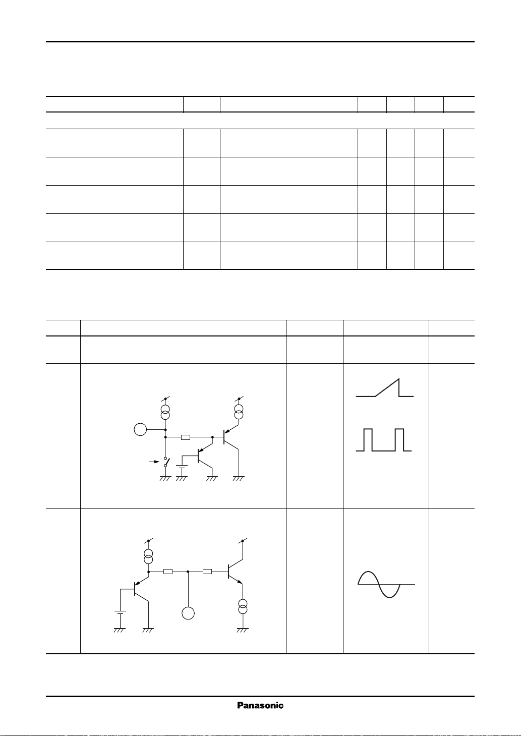
■ Terminal Equivalent Circuits
Pin No. Equivalent circuit Impedance Signal waveform DC (V)
1V
CC
Input 15, output 13 −3 +3dB
AD
VIN = pin 15, 200 mV[p-p]
Input 15, output 13 1.7 dB
ENON
VIN = pin 15, 200 mV[p-p]
Input 16, output 13 0.4 µs
VIN = rectangular wave, 0 V to 5 V 300 Hz
Input 16, output 13 570 µs
VIN = rectangular wave, 0 V to 5 V 300 Hz
Input 16, output 13 80
HSON
VIN = triangular wave, 2 V[p-p] 300 Hz
5.0
mV[p-p]
2 HMW Current output
2
200 Ω
HSS on
3 RA IN (CA) 10 kΩ 2.3
10 kΩ 200 Ω
Sin wave
3
5
 Loading...